|
|
|
PDF TB62D901FNG Data sheet ( Hoja de datos )
| Número de pieza | TB62D901FNG | |
| Descripción | AC/DC Step-Down Conversion Type LED Lighting Driver | |
| Fabricantes | Toshiba | |
| Logotipo | ||
Hay una vista previa y un enlace de descarga de TB62D901FNG (archivo pdf) en la parte inferior de esta página. Total 23 Páginas | ||
|
No Preview Available !
TOSHIBA BiCD Integrated Circuit Silicon Monolithic
TB62D901FNG
TB62D901FNG
AC/DC Step-Down Conversion Type LED Lighting Driver
1. General
The TB62D901FNG is a constant current driver IC ideal for
use in the step-down AC/DC conversion type LED lighting
applications.
The TB62D901FNG features architecture with automatic Off
time adjustment control that can be used to achieve minimum
LED current variations by the effect of fluctuated input voltage
or change of LED forward voltage.
The device allows linear dimming or PWM dimming. It has
extensive detection functions that are thermal shutdown,
over-current detection, over-voltage detection, under-voltage
lockout, and current sensing input terminal (ISEN1) open
detection.
2. Application
LED lighting
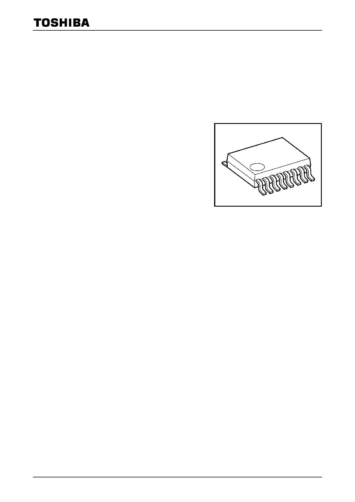
TB62D901FNG
SSOP16-P-225-0.65B
Weight: 0.07 g (typ.)
3. Features
• Operating supply voltage
• Dimming function
• Switching frequency
• Operation mode
• Efficiency
• Detection function
• IC standby function
• Operating temperature
• Package
: 12V to 30V
: Linear dimming (by adjustment of LED peak current)
PWM dimming
: Adjustable of up to 500kHz (MAX)
: Current continuous conduction mode
(Automatic OFF time control mode, Fixed off time mode)
Critical conduction mode
: 90% or more with recommended components
: Thermal shutdown (TSD)
: Over-current detection (OCP)
: Over-voltage detection (OVP)
: Under-voltage lockout (UVLO)
: ISEN terminal open detection (IOP)
: EN signal allows standby mode with 0.8mA (MAX) consumption
current
: Topr = −40 °C to 105 °C
: SSOP16-P-225-0.65B
1 2012-03-12
1 page 
8. Absolute Maximum Ratings (Ta = 25°C)
Characteristics
Symbol
Supply voltage
Input pin voltage (PWMD, LD, RC, EN,
and MS)
VREG pin voltage
Feedback pin voltage
(ISEN1 and VSEN)
GATE pin voltage
Operating temperature
Storage temperature
Thermal resistance
VCC
VIN
VREG
VFB
VGATE
Topr
Tstg
Rth(j-a)
Power dissipation
PD
Rating Note1
−0.3 to 40
−0.3 to 6.0
−0.3 to 6.0
−0.3 to 6.0
−0.3 to VCC
−40 to 105
−55 to 150
87.3* Note 2
1.43* Note2,3
TB62D901FNG
Unit
V
V
V
V
V
°C
°C
°C/ W
W
Note1: Voltage is PGND/GND/ISEN2 referenced.
Note2: PCB condition is 76.2×114.3×1.6mm (JEDEC 4 layer substrate)
Note3: When ambient temperature is 25°C or more. Every time ambient temperature exceeded 1°C, please decrease 1/Rth(j-a).
9. Operating Condition (Unless otherwise noted, Ta = -40 to 105 °C)
Characteristics
Operating supply voltage
Switching frequency
LD pin input voltage
RC pin input voltage
VSEN pin input voltage
Symbol
VCC
fSW
VLD1
VLD2
VRC1
VRC2
VVSEN1
VVSEN2
Test Conditions
When LED peak current adjustment
function is used
When LED peak current adjustment
function is not used
When LED peak current adjustment
function is used
When LED peak current adjustment
function is not used
When using it in automatic OFF time
control mode
When using it in Fixed OFF time mode
Min
12
―
0.2
4.5
1
0
0.5
4.5
Typ.
―
―
―
―
―
―
―
―
Max
30
500
3.8
VREG
4.0
0.5
3
VREG
Unit
V
kHz
V
V
V
GATE pin output voltage which is the same level as VCC. Please set up VCC in consideration of the Absolute Maximum Ratings of
the external power MOSFET
5 2012-03-12
5 Page 
TB62D901FNG
12. Dimming function
This TB62D901FNG incorporates three kinds of dimming function.
Operation mode
1 PWM Dimming
2 Linear Dimming
3 Ripple Dimming
Control Methods
Input Pin
Signal Type
PWMD
LD
RC
Digital signals
Analogue voltage
Analog voltage
Table1 2 Dimming Control Mode Comparison
LED current
Dimming Results
Peak current Ripple current value
PWMD=H: ON
PWMD=L: OFF
Fixed
Fixed
ON Change
Fixed
ON Fixed Changed
12.1 PWM dimming
The LED current is turned on and off according to the PWM signal input to the PWMD input pin.
When this function is not used, please connect PWMD to the VREG pin.
PWM signal
ILED
Figure 5 PWM Dimming
12.2 Linear Dimming
This is a linear dimming by controlling the peak current of LED.
The peak current of LED is controlled by VLD the analog voltage applied to the LD pin from which an internal
voltage VPEAK is derived to the input of an internal comparator. The comparator to compare VPEAK and the voltage
from input ISEN1 of the current sensing resistor RSET. VPEAK is determined by method of applied voltage to LD
pin.
Table 3 VPEAK setting
Input voltage to LD pin VLD
The LD and the VREG pins are shorten together.
(When not using linear dimming by LD input)
The analog voltage is applied to LD pin.
VPEAK
1.0V(TYP.)
VLD/1.5(TYP.)
(VLD needs to be in the range of 0.2V to 3.8V)
.
VPEAK vs VLD
3
2.5
VLD 2
1.5
1
0.5
ILED 0
0
(a) Waveform of LED current vs control voltage VLD
0.5 1 1.5 2 2.5 3 3.5 4 4.5
VLD (V)
(b) The relation between VPEAK and VLD
5
Figure 6 Linear Dimming
5.5
11 2012-03-12
11 Page | ||
| Páginas | Total 23 Páginas | |
| PDF Descargar | [ Datasheet TB62D901FNG.PDF ] | |
Hoja de datos destacado
| Número de pieza | Descripción | Fabricantes |
| TB62D901FNG | AC/DC Step-Down Conversion Type LED Lighting Driver | Toshiba |
| Número de pieza | Descripción | Fabricantes |
| SLA6805M | High Voltage 3 phase Motor Driver IC. |
Sanken |
| SDC1742 | 12- and 14-Bit Hybrid Synchro / Resolver-to-Digital Converters. |
Analog Devices |
|
DataSheet.es es una pagina web que funciona como un repositorio de manuales o hoja de datos de muchos de los productos más populares, |
| DataSheet.es | 2020 | Privacy Policy | Contacto | Buscar |