|
|
PDF NX3L1G66 Data sheet ( Hoja de datos )
| Número de pieza | NX3L1G66 | |
| Descripción | Low-voltage analog switch | |
| Fabricantes | NXP Semiconductors | |
| Logotipo | ||
Hay una vista previa y un enlace de descarga de NX3L1G66 (archivo pdf) en la parte inferior de esta página. Total 16 Páginas | ||
|
No Preview Available !
NX3L1G66
Low-voltage analog switch
Rev. 01 — 3 January 2008
Product data sheet
www.datasheet4u.com
1. General description
The NX3L1G66 provides one single pole, single-throw analog switch function. It has two
input/output terminals (Y and Z) and an active HIGH enable input pin (E). When E is LOW,
the analog switch is turned off.
Schmitt trigger action at the enable input (E) makes the circuit tolerant to slower input rise
and fall times across the entire VCC range from 1.4 V to 3.6 V.
The NX3L1G66 allows signals with amplitude up to VCC to be transmitted from Y to Z; or
from Z to Y. Its low ON resistance (0.5 Ω) and flatness (0.13 Ω) ensures minimal
attenuation and distortion of transmitted signals.
2. Features
s Wide supply voltage range from 1.4 V to 3.6 V
s Very low ON resistance (peak):
x 1.6 Ω (typical) at VCC = 1.4 V
x 1.0 Ω (typical) at VCC = 1.65 V
x 0.55 Ω (typical) at VCC = 2.3 V
x 0.50 Ω (typical) at VCC = 2.7 V
s High noise immunity
s ESD protection:
x HBM JESD22-A114E Class 3A exceeds 7500 V
x MM JESD22-A115-A exceeds 200 V
x CDM AEC-Q100-011 revision B exceeds 1000 V
s CMOS low-power consumption
s Latch-up performance exceeds 100 mA per JESD 78 Class II Level B
s Direct interface with TTL levels at 3.0 V
s Control input accepts voltages above supply voltage
s High current handling capability (350 mA continuous current under 3.3 V supply)
s Specified from −40 °C to +85 °C and from −40 °C to +125 °C
3. Applications
s Cell phone
s PDA
s Portable media player
1 page 
NXP Semiconductors
NX3L1G66
Low-voltage analog switch
11.1 Test circuits
www.datasheet4u.com
VCC
VIL E
IS Z
VI
Y IS
GND
VO
VIH E
IS Z
VI
VCC
Y
GND
VO
001aag488
VI = 0.3 V or VCC − 0.3 V; VO = VCC − 0.3 V or 0.3 V.
Fig 4. Test circuit for measuring OFF-state leakage
current
001aag489
VI = 0.3 V or VCC − 0.3 V; VO = open circuit.
Fig 5. Test circuit for measuring ON-state leakage
current
11.2 ON resistance
Table 8. ON resistance
At recommended operating conditions; voltages are referenced to GND (ground = 0 V); for graphs see Figure 7 to Figure 12.
Symbol Parameter
Conditions
−40 °C to +85 °C −40 °C to +125 °C Unit
Min Typ[1] Max
Min
Max
RON(peak) ON resistance (peak)
VI = GND to VCC;
ISW = 100 mA;
see Figure 6
RON(flat)
ON resistance (flatness)
VCC = 1.4 V
VCC = 1.65 V
VCC = 2.3 V
VCC = 2.7 V
VI = GND to VCC;
ISW = 100 mA
VCC = 1.4 V
VCC = 1.65 V
VCC = 2.3 V
VCC = 2.7 V
-
-
-
-
[2]
1.6 3.7
1.0 1.6
0.55 0.8
0.5 0.75
- 1.0 3.3
- 0.5 1.2
- 0.15 0.3
- 0.13 0.3
-
-
-
-
-
-
-
-
4.1 Ω
1.7 Ω
0.9 Ω
0.9 Ω
3.6 Ω
1.3 Ω
0.35 Ω
0.35 Ω
[1] Typical values are measured at Tamb = 25 °C.
[2] Flatness is defined as the difference between the maximum and minimum value of ON resistance measured at identical VCC and
temperature.
NX3L1G66_1
Product data sheet
Rev. 01 — 3 January 2008
© NXP B.V. 2008. All rights reserved.
5 of 16
5 Page 
NXP Semiconductors
NX3L1G66
Low-voltage analog switch
www.datasheet4u.com
0.5VCC
RL VIL E
Y/Z
VCC
0.5VCC
RL
Z/Y
fi dB
Adjust fi voltage to obtain 0 dBm level at input.
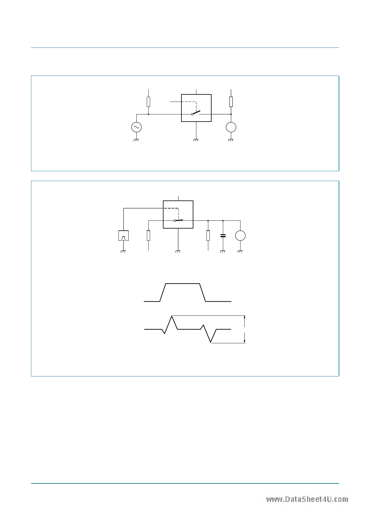
Fig 17. Test circuit for measuring isolation (OFF-state)
001aah380
a. Test circuit
G VI
VCC
E
Y/Z Z/Y
RL RL CL V VO
0.5VCC
0.5VCC
001aah383
logic
input (E)
off
on
off
VO Vct
001aah381
b. Input and output pulse definitions
Fig 18. Test circuit for measuring crosstalk voltage between digital inputs and switch
NX3L1G66_1
Product data sheet
Rev. 01 — 3 January 2008
© NXP B.V. 2008. All rights reserved.
11 of 16
11 Page | ||
| Páginas | Total 16 Páginas | |
| PDF Descargar | [ Datasheet NX3L1G66.PDF ] | |
Hoja de datos destacado
| Número de pieza | Descripción | Fabricantes |
| NX3L1G66 | Low-voltage analog switch | NXP Semiconductors |
| Número de pieza | Descripción | Fabricantes |
| SLA6805M | High Voltage 3 phase Motor Driver IC. |
Sanken |
| SDC1742 | 12- and 14-Bit Hybrid Synchro / Resolver-to-Digital Converters. |
Analog Devices |
|
DataSheet.es es una pagina web que funciona como un repositorio de manuales o hoja de datos de muchos de los productos más populares, |
| DataSheet.es | 2020 | Privacy Policy | Contacto | Buscar |
