|
|
PDF L9610C Data sheet ( Hoja de datos )
| Número de pieza | L9610C | |
| Descripción | PWM POWER MOS CONTROLLER | |
| Fabricantes | STMicroelectronics | |
| Logotipo |  |
|
Hay una vista previa y un enlace de descarga de L9610C (archivo pdf) en la parte inferior de esta página. Total 12 Páginas | ||
|
No Preview Available !
L9610C
L9611C
PWM POWER MOS CONTROLLER
. HIGH EFFICIENCY DUE TO PWM CONTROL
AND POWERMOS DRIVER
. LOAD DUMP PROTECTION
. LOAD POWER LIMITATION
. EXTERNAL POWERMOS PROTECTION
. LIMITED OUTPUT VOLTAGE SLEW RATE
DE SCR I P TI O N
The L9610C/11C is a monolithic integrated circuit
working in PWM mode as controller of an external
powerMOS transistor in High Side Driver configura-
tion.
Features of the device include controlled slope of
the leading and trailing edge of the gate driving vol-
tage, linear current limiting with protection timer, set-
table switching frequencyfo, TTL compatible enable
function, protection status ouput pin. The device is
mounted in SO16 micropackage, and DIP16 pack-
age.
SO16
DIP 16
ORDERING NUMBERS: L9610C
L9611C
BLOCK DIAGRAM
November 1991
1/9
This is advanced information on a new product now in development or undergoing evaluation. Details are subject to change without notice.
1 page 
L9610C - L9611C
After the overcurrent protection time is reached, the
powerMOS is switched-off ; this condition is latched
by setting an internal flip-flop and is externallymoni-
tored by the low state of the MON pin.
To resetthe latch the supply voltage hasto fall below
VSL or the device must be switched off.
UNDER AND OVERVOLTAGE SENSE WITH
LOAD DUMP PROTECTION
The undervoltage detection feature resets the timer
and switches off the output driving signal when the
supply voltage is less than VSL.
If the supply voltage exceeds the max operating
supply voltage value, an internal comparator dis-
ables the charge pump, the oscillator and the exter-
nal powerMOS.
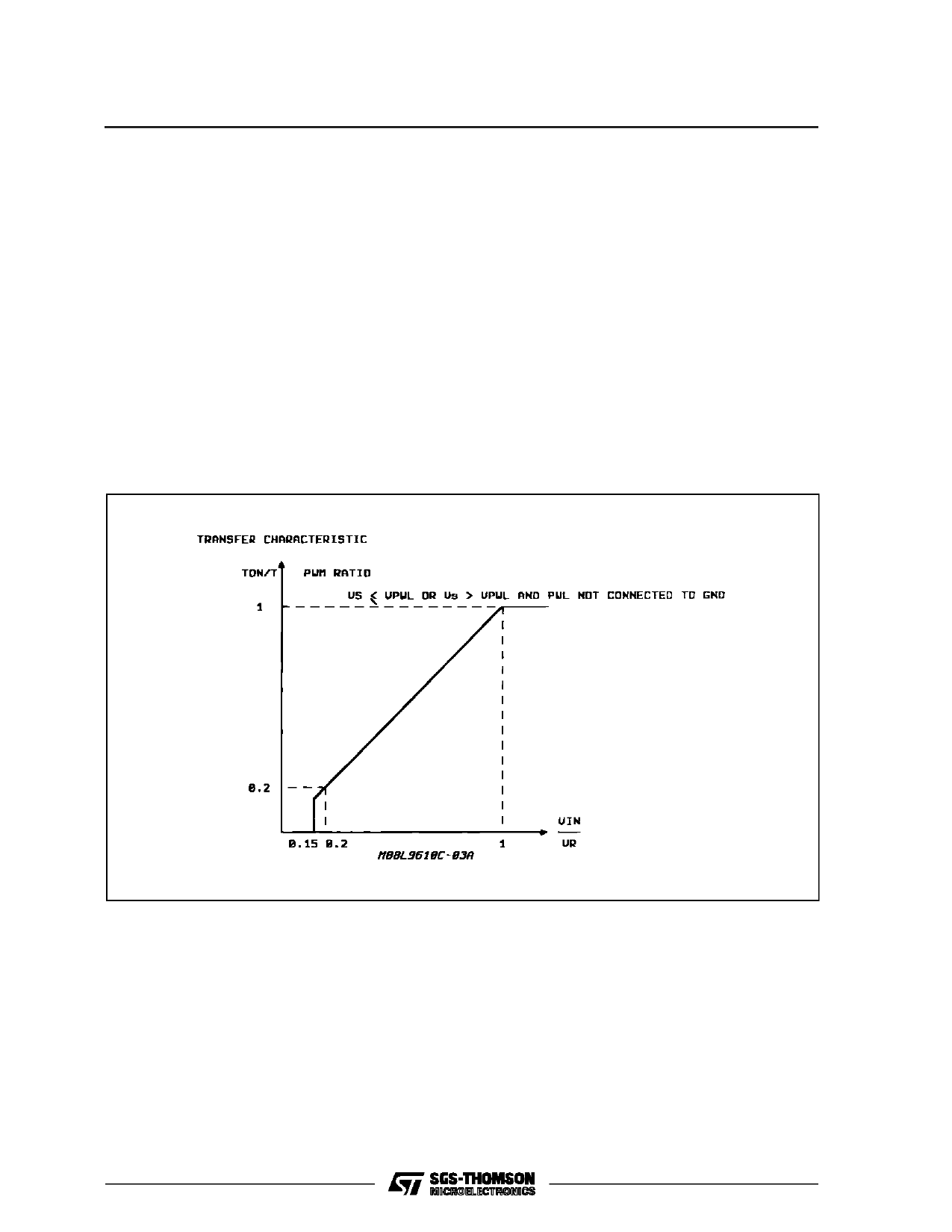
Figure 1 : Typical Transfer Curve.
In both cases the thresholds are provided with suit-
able hysteresis values.
The load dump protection function allows the device
to withstand - for a limited time - high overvoltages.
It consists of an active clamping diode which limits
the circuit supply voltage to VCLAMP and an external
current limiting resistor R1. The maximum pulse
supply current (see abs. max. ratings is equal to
0.3A. Therefore the maximum load dump voltage is
given by :
VDUMP = VSC + 0.3R1
In this condition the gate of the powerMOS is held
at the GND pin potential and thus the load voltage
is :
VL = Vs - VCLAMP - VGS
5/12
5 Page 
DIM.
A
a1
a2
b
b1
C
c1
D
E
e
e3
F
L
M
S
MIN.
0.1
0.35
0.19
9.8
5.8
3.8
0.4
mm
TYP.
0.5
1.27
8.89
MAX.
1.75
0.25
1.6
0.46
0.25
MIN.
0.004
0.014
0.007
45 (typ.)
10 0.386
6.2 0.228
4.0 0.150
1.27 0.016
0.62
8 (max.)
L9610C - L9611C
inch
TYP.
0.020
0.050
0.350
MAX.
0.069
0.009
0.063
0.018
0.010
0.394
0.244
0.157
0.050
0.024
11/12
11 Page | ||
| Páginas | Total 12 Páginas | |
| PDF Descargar | [ Datasheet L9610C.PDF ] | |
Hoja de datos destacado
| Número de pieza | Descripción | Fabricantes |
| L9610 | PWM POWER MOS CONTROLLER | STMicroelectronics |
| L9610C | PWM POWER MOS CONTROLLER | STMicroelectronics |
| Número de pieza | Descripción | Fabricantes |
| SLA6805M | High Voltage 3 phase Motor Driver IC. |
Sanken |
| SDC1742 | 12- and 14-Bit Hybrid Synchro / Resolver-to-Digital Converters. |
Analog Devices |
|
DataSheet.es es una pagina web que funciona como un repositorio de manuales o hoja de datos de muchos de los productos más populares, |
| DataSheet.es | 2020 | Privacy Policy | Contacto | Buscar |
