|
|
|
PDF VNI8200XP-32 Data sheet ( Hoja de datos )
| Número de pieza | VNI8200XP-32 | |
| Descripción | Octal high-side smart power solid-state relay | |
| Fabricantes | STMicroelectronics | |
| Logotipo | ||
Hay una vista previa y un enlace de descarga de VNI8200XP-32 (archivo pdf) en la parte inferior de esta página. Total 30 Páginas | ||
|
No Preview Available !
VNI8200XP-32
Octal high-side smart power solid-state relay with serial/parallel
selectable interface on-chip
Datasheet - production data
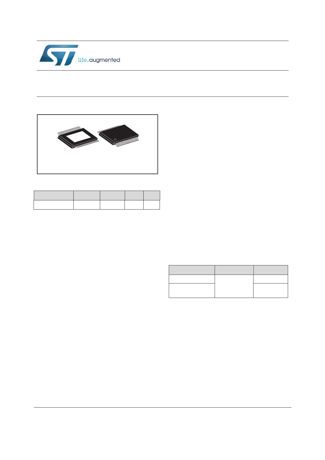
PowerSSO-36 package
with exposed pad down (EPD)
Features
Type
VNI8200XP-32
Vdemag(1)
VCC-45 V
RDS(on)(1)
0.11 Ω
IOUT(1)
1A
VCC
45 V
Notes:
(1)Per channel
Output current: 1 A per channel
Serial/parallel selectable interface
Short-circuit protection
8-bit and 16-bit SPI interface for IC
command and control diagnostic
Channel overtemperature detection and
protection
Thermal independence of separate channels
All type of loads (resistive, capacitive,
inductive load) are driven
Loss of GND protection
Power Good diagnostic
Undervoltage shutdown with hysteresis
Overvoltage protection (VCC clamping)
Very low supply current
Common fault open drain output
IC warning temperature detection
Channel output enable
100 mA high efficiency step-down switching
regulator with integrated boot diode
Adjustable regulator output
Switching regulator disable
5 V and 3.3 V compatible I/Os
Channel output status LED driving 4x2
multiplexed array
Fast demagnetization of inductive loads
ESD protection
Designed to meet IEC61131-2,
IEC61000-4-4 and IEC61000-4-5
Applications
Programmable logic control
Industrial PC peripheral input/output
Numerical control machines
Table 1: Device summary
Order code
Package
Packing
VNI8200XP-32
PowerSSO-36
VNI8200XPTR-32
Tube
Tape and
reel
August 2015
DocID027849 Rev 3
This is information on a product in full production.
1/43
www.st.com
1 page 
VNI8200XP-32
List of figures
List of figures
Figure 1: Block diagram ..............................................................................................................................7
Figure 2: Pin connection (top view) ............................................................................................................8
Figure 3: Reverse polarity protection........................................................................................................17
Figure 4: Maximum demagnetization energy vs. load current, typical values ..........................................18
Figure 5: SPI mode diagram .....................................................................................................................21
Figure 6: Output channel enable/disable behavior ...................................................................................22
Figure 7: Power Good diagnostic .............................................................................................................23
Figure 8: Watchdog reset .........................................................................................................................24
Figure 9: LED driving array .......................................................................................................................27
Figure 10: Typical circuit for switching regulation VDC-out = 3.3 V .............................................................29
Figure 11: Typical circuit for switching regulation VDC-out = 5 V ................................................................30
Figure 12: SPI directional logic convention...............................................................................................31
Figure 13: PowerSSO-36 thermal impedance vs. time ............................................................................32
Figure 14: Thermal behavior.....................................................................................................................33
Figure 15: Serial timing .............................................................................................................................34
Figure 16: dV/dt(ON) and dV/dt(OFF) time diagram test conditions ........................................................35
Figure 17: td(ON) and td(OFF) time diagram test conditions...........................................................................35
Figure 18: PowerSSO-36 package outline ...............................................................................................36
Figure 19: PowerSSO-36 package outline details ....................................................................................37
Figure 20: PowerSSO-36 package outline details (section B-B) ..............................................................37
Figure 21: PowerSSO-36 tube shipment outline ......................................................................................39
Figure 22: PowerSSO-36 tape dimension outline ....................................................................................40
Figure 23: PowerSSO-36 reel shipment outline .......................................................................................41
DocID027849 Rev 3
5/43
5 Page 
VNI8200XP-32
Symbol
Rth(JC)
Rth(JA)
Table 4: Thermal data
Parameter
Thermal resistance junction-case (1)
Thermal resistance junction-ambient (2)
Max.
Max.
Maximum ratings
Value
2
15
Unit
°C/W
°C/W
Notes:
(1)Per channel.
(2)PowerSSO-36 mounted on a four-layer FR4, with 8 cm2 for each layer, Cu thickness = 35 µm
DocID027849 Rev 3
11/43
11 Page | ||
| Páginas | Total 30 Páginas | |
| PDF Descargar | [ Datasheet VNI8200XP-32.PDF ] | |
Hoja de datos destacado
| Número de pieza | Descripción | Fabricantes |
| VNI8200XP-32 | Octal high-side smart power solid-state relay | STMicroelectronics |
| Número de pieza | Descripción | Fabricantes |
| SLA6805M | High Voltage 3 phase Motor Driver IC. |
Sanken |
| SDC1742 | 12- and 14-Bit Hybrid Synchro / Resolver-to-Digital Converters. |
Analog Devices |
|
DataSheet.es es una pagina web que funciona como un repositorio de manuales o hoja de datos de muchos de los productos más populares, |
| DataSheet.es | 2020 | Privacy Policy | Contacto | Buscar |