|
|
PDF IR11688S Data sheet ( Hoja de datos )
| Número de pieza | IR11688S | |
| Descripción | DUAL SYNCHRONOUS RECTIFICATION CONTROL IC | |
| Fabricantes | Infineon | |
| Logotipo |  |
|
Hay una vista previa y un enlace de descarga de IR11688S (archivo pdf) en la parte inferior de esta página. Total 27 Páginas | ||
|
No Preview Available !
SMPS IC
SmartrectifierTM
IR11688S
DUAL SYNCHRONOUS RECTIFICATION CONTROL IC
Features
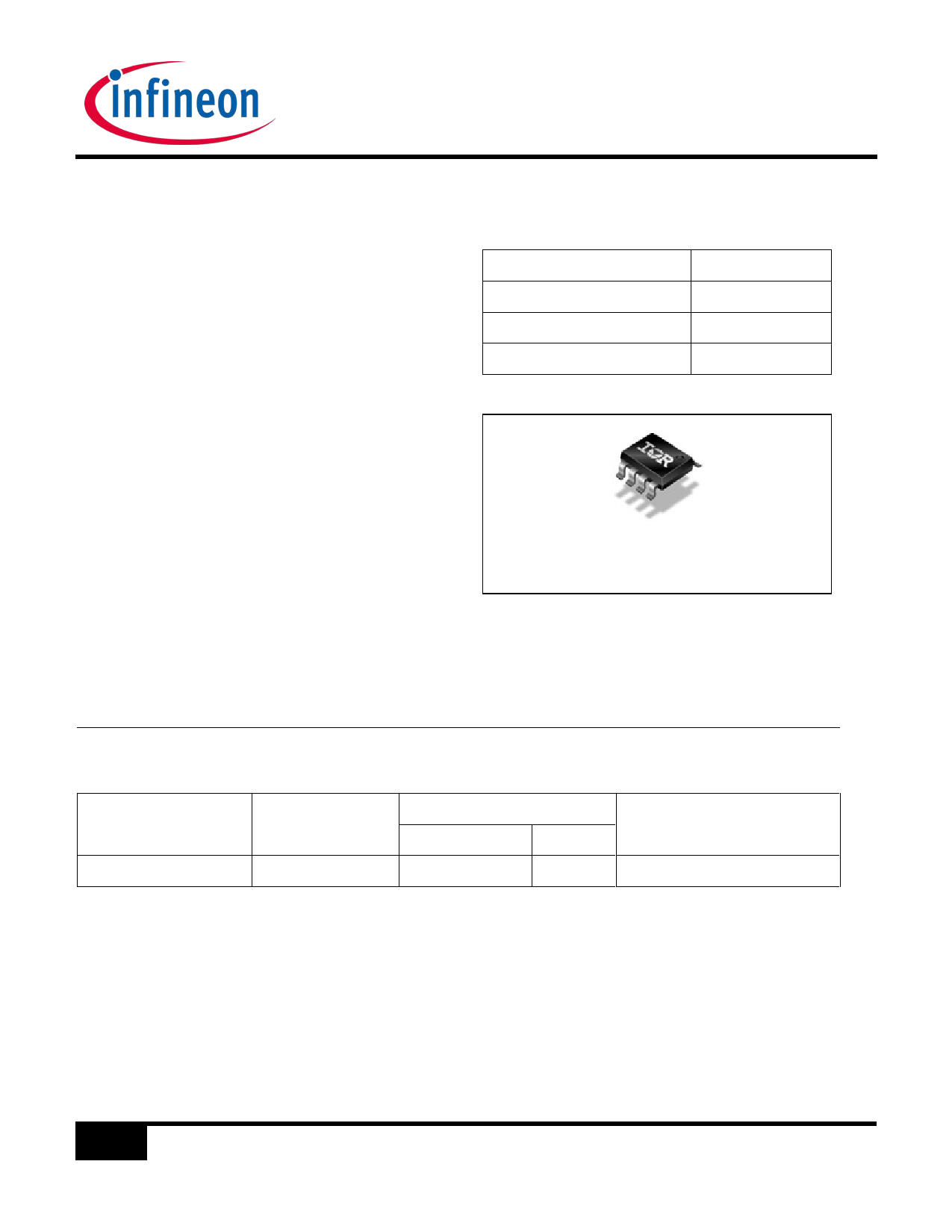
Product Summary
• Secondary-side high speed synchronous
rectification controller for resonant half bridge
Topology
LLC Half-bridge
converters
VD
• Direct sensing of MOSFET drain voltage up to 200V
• Operates up to 400kHz switching frequency
VOUT
200V
Vcc
• Programmable Minimum On Time
• Anti-bounce logic and UVLO protection
Io+ & I o-
+1A & -4A
•
Linear turn-off phase to compensate for premature
switch off due to parasitic inductance
Package Options
• 4A peak turn off drive current
• Micropower start-up & ultra-low quiescent current
• 50ns turn-off propagation delay
• Wide Vcc operating range 4.75V to 18V
• Cycle by Cycle MOT Protection
• Auto low power mode standby mode
• Improved noise immunity
• Compatible with Energy Star low standby power
8-Pin SOIC
• Lead-free
Typical Applications
• Desktop SMPS, Server SMPS, AC-DC adapters,
LCD & PDP TV, Telecom SMPS
Ordering Information
Base Part Number
Package Type
IR11688S
SOIC8N
Standard Pack
Form
Quantity
Tape and Reel
2500
Complete Part Number
IR11688STRPBF
1 2016-1-18
1 page 
IR11688S
Absolute Maximum Ratings
Absolute maximum ratings indicate sustained limits beyond which damage to the device may occur. All voltage
parameters are absolute voltages referenced to COM, all currents are defined positive into any pin. The thermal
resistance and power dissipation ratings are measured under board mounted and still air conditions.
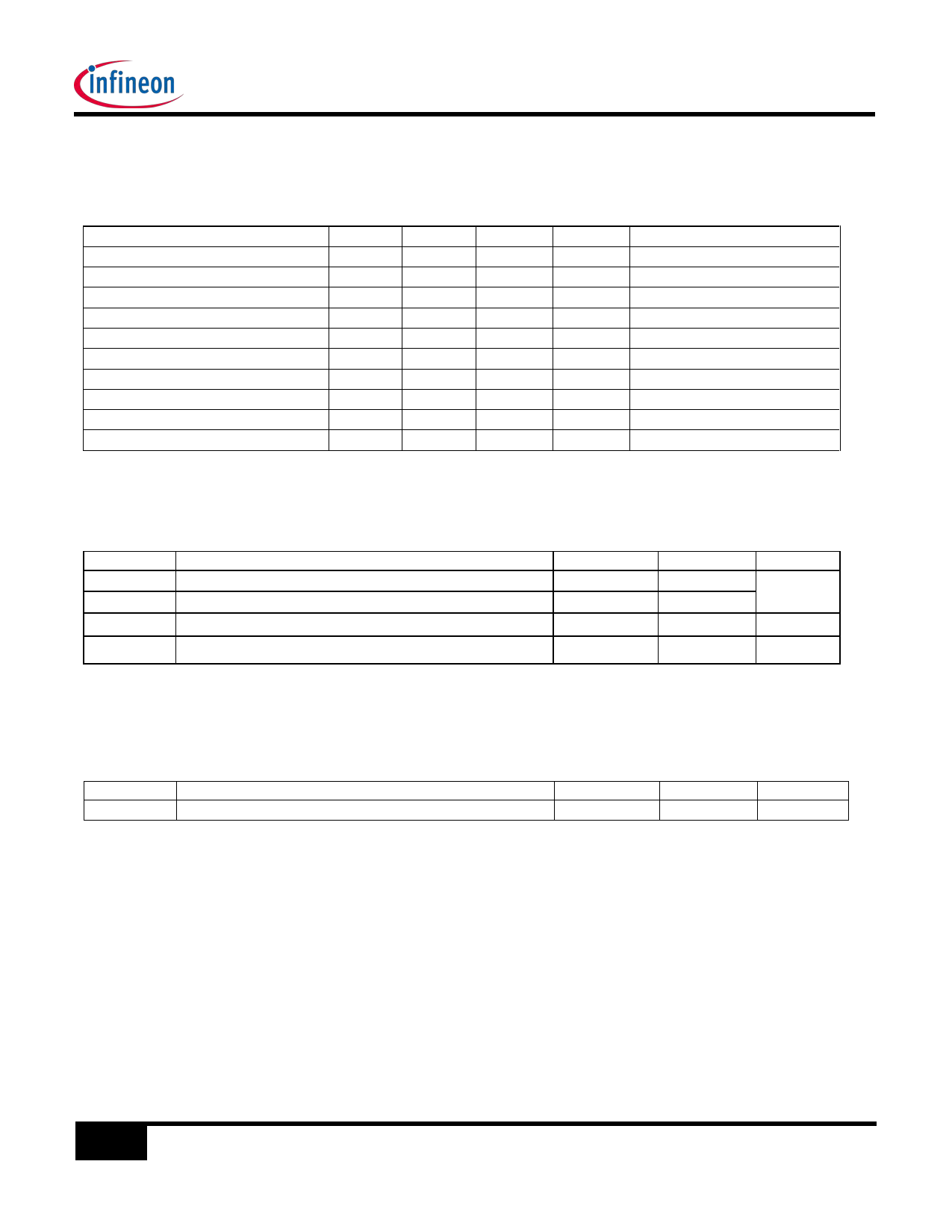
Parameters
Supply Voltage
Cont. Drain Sense Voltage
Pulse Drain Sense Voltage
Source Sense Voltage
Gate Voltage
MOT Voltage
Operating Junction Temperature
Storage Temperature
Thermal Resistance
Package Power Dissipation
Symbol
VCC
VD1,2
VD1,2
VS
VGATE1,2
VMOT
TJ
TS
RθJA
PD
Min.
-0.3
-1
-3
-1
-0.3
-0.3
-40
-55
Max.
20
200
200
5
Vcc+0.3
3.5
150
150
128
970
Units
V
V
V
V
V
V
°C
°C
°C/W
mW
Remarks
SOIC-8
SOIC-8, TAMB=25°C
Recommended Operating Conditions
For proper operation the device should be used within the recommended conditions.
Symbol
VCC
VD
TJ
Definition
Supply voltage
Drain Sense Voltage
Junction Temperature
Min.
4.75
-3 ①
-40
Fsw Switching Frequency
---
Max.
18
200
125
400
① VD -3V negative spike width ≤100ns
Recommended Component Values
Symbol
Component
RMOT
MOT pin resistor value
Min.
20
Max.
150
Units
V
°C
kHz
Units
kΩ
5 2016-1-18
5 Page 
IR11688S
Detailed Pin Description
VCC: Power Supply
This is the supply voltage pin of the IC, monitored by the under voltage lockout circuit. It is possible to turn off the
IC entering UVLO mode by pulling this pin below the minimum turn off threshold voltage for micro power
consumption.
To prevent noise interfering with operation, a ceramic decoupling capacitor should be connected from Vcc to GND
and located as close to the IC as possible. A low value series resistor may also be added to the Vcc supply circuit
for filtering if required. Vcc is internally clamped at around 20V.
GND: Ground
This is power ground connection to the IC. Internal circuit blocks and gate drivers are referenced to this point.
MOT: Minimum On Time
The MOT programming pin controls the amount of minimum on time. Once VTH2 is crossed at either VD input, the
corresponding gate drive output will transition high to turn on the SR MOSFET. Spurious ringing and oscillations
can falsely trigger the input comparator to prematurely switch the output off. During the MOT period the input
comparator is disabled maintaining conduction through the MOSFET on for this preset minimum period.
The MOT is typically programmed between 500ns and 2us by means of an external resistor referenced to GND.
VD1 and VD2: Drain Voltage Sense
The VD pins are the voltage sensing inputs for the SR MOSFET drains. These are high voltage inputs therefore
particular care must be taken in properly routing the connections. Additional RC filters can be placed at these
inputs to improve noise immunity, however only a small resistor (≤1kΩ) and capacitor value (in the pF range) may
be used to avoid introducing excessive delay to the control input.
VS: Source Voltage Sense
This is the signal ground for the sources of the two SR power MOSFETs to provide an accurate differential voltage
measurement. Kelvin connect this pin to the source of MOSFET2 (channel 2 MOSFET) is recommended if the two
MOSFETs are far apart to each other.
GATE1 and GATE2: Gate Drive Outputs
Each gate driver output has +1A/-4A peak drive capability. Although these pins can be directly connected to the
SR MOSFET gates the use of gate resistors is recommended, especially when using several MOSFETs in parallel.
Care must be taken to keep the gate loop as short and as tight as possible in order to achieve optimal switching
performance.
11 2016-1-18
11 Page | ||
| Páginas | Total 27 Páginas | |
| PDF Descargar | [ Datasheet IR11688S.PDF ] | |
Hoja de datos destacado
| Número de pieza | Descripción | Fabricantes |
| IR11688S | DUAL SYNCHRONOUS RECTIFICATION CONTROL IC | Infineon |
| Número de pieza | Descripción | Fabricantes |
| SLA6805M | High Voltage 3 phase Motor Driver IC. |
Sanken |
| SDC1742 | 12- and 14-Bit Hybrid Synchro / Resolver-to-Digital Converters. |
Analog Devices |
|
DataSheet.es es una pagina web que funciona como un repositorio de manuales o hoja de datos de muchos de los productos más populares, |
| DataSheet.es | 2020 | Privacy Policy | Contacto | Buscar |
