|
|
|
PDF LD5532 Data sheet ( Hoja de datos )
| Número de pieza | LD5532 | |
| Descripción | Green-Mode PWM Controller | |
| Fabricantes | Leadtrend Technology | |
| Logotipo | ||
Hay una vista previa y un enlace de descarga de LD5532 (archivo pdf) en la parte inferior de esta página. Total 18 Páginas | ||
|
No Preview Available !
LD5532
07/08/2014
Green-Mode PWM Controller with Frequency Swapping and
Audio Noise Prevention
REV. 00
General Description
The LD5532 is built with several functions, audio noise
prevention, protection and EMI-improved solution in a tiny
package. It takes less components counts or circuit space,
especially ideal for those total solutions of low cost.
It includes low startup current, green-mode power-saving
operation, leading-edge blanking of the current sense and
internal slope compensation. It also features protections
of OLP (Over Load Protection) and OVP (Over Voltage
Protection) to prevent circuit from damage under
abnormal conditions.
Furthermore, the Frequency Swapping function is also
built-in to reduce the noise level and thus helps the power
circuit designers to easily deal with the EMI filter design by
spending minimum amount of component cost and
developing time.
Features
High-Voltage CMOS Process with Excellent ESD
protection
Very Low Startup Current (<1.5A)
Current Mode Control
Green Mode Control
UVLO (Under Voltage Lockout)
LEB (Leading-Edge Blanking) on CS Pin
Internal Frequency Swapping
Internal Slope Compensation
OVP (Over Voltage Protection) on Vcc Pin
Brownout Protection
OLP (Over Load Protection)
300mA/-500mA Driving Capability
Grouping Frequency Limitation for Audio Noise
Applications
LCD Monitor/TV Power
Switching AC/DC Adaptor
Open Frame Switching Power Supply
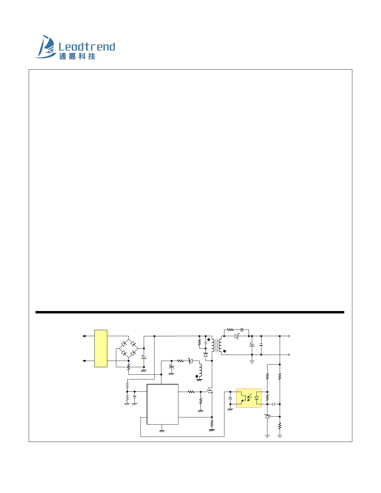
Typical Application
AC
input
EMI
Filter
DC
Output
BNO
VCC
OUT
COMP
LD5532
GND
CS
Leadtrend Technology Corporation
LD5532-DS-00 July 2014
1
www.leadtrend.com.tw
photocoupler
1 page 
Electrical Characteristics
(TA = +25C unless otherwise stated, VCC=15.0V)
PARAMETER
CONDITIONS
Supply Voltage (Vcc Pin)
Startup Current
VCOMP=0V
Operating Current
(with 1nF load on OUT pin)
VCOMP=3V
OLP Tripped
OVP Tripped
UVLO (off)
UVLO (on)
OVP Level
Voltage Feedback (Comp Pin)
Short Circuit Current
Open Loop Voltage
VCOMP=0V
COMP pin open
Fixed Frequency Mode Threshold
VCOMP(*)
Green Mode Threshold VCOMP(*)
Burst Mode Threshold VCOMP
Current Sensing (CS Pin)
Maximum Input Voltage, VCS_Off
Minimum Input Voltage, VCS_min
Top Compensation Duty Ratio
Bottom Compensation Duty Ratio
Leading Edge Blanking Time
Inter Slope Compensation
Input impedance
Delay to Output
Hysteresis
0% to DMAX.
(Linearly increase)
LD5532
Symbol MIN TYP MAX UNITS
ISTUP
IVCC_0V
IVCC_3V
IOLP
IOVP
VUVLO(OFF)
VUVLO(ON)
VOVP
0.1
0.55
1.62
7.5
15
25
0.4
0.625
1.80
0.490
0.490
8.5
16
26
1
0.675
1.98
9.5
17
27
A
mA
mA
mA
mA
V
V
V
ICOMP_0V
VCOMP_OP
VCOMP_F
VCOMP_GN
VBURST
VBURST_H
0.16
5.00
0.18
5.20
2.20
2.00
1.65
100
0.20
5.40
mA
V
V
V
V
mV
VCS_OFF
VCS_MIN
DTOP
DBOM
TLEB
VSLOPE
ZIN
TD
0.80
0.6
49
17.7
285
1
50
0.85
0.65
51.6
18.6
250
300
--
100
0.90
0.7
54
19.5
315
10
150
V
V
%
%
nS
mV
M
nS
Leadtrend Technology Corporation
LD5532-DS-00 July 2014
5
www.leadtrend.com.tw
5 Page 
LD5532
sensing pin is set at 0.85V. From above, the MOSFET peak
current can be obtained from below.
IPEAK(MAX )
0.85V
RS
Vin
Output Stage and Maximum Duty-Cycle
An output stage of a CMOS buffer, with typical 300mA
driving capability, is incorporated to drive a power MOSFET
directly. And the maximum duty-cycle of LD5532 is limited
to 75% to avoid the transformer saturation.
Cbulk
AC
Line
R1
D1
C1
VCC
OUT
LD5532
Comp
CS
GND
Fig. 19
Rs
Voltage Feedback Loop
The voltage feedback signal is provided from the TL431 at
the secondary side through the photo-coupler to the COMP
pin of the LD5532. Similar to UC3842, the LD5532 would
carry a diode voltage offset at the stage to feed the voltage
divider at the ratio of 2RB and RB, that is,
V(PWM COMPARATOR
)
RB
2RB RB
(VCOMP
VF )
A pull-high resistor is embedded internally and can be
eliminated externally.
A 250nS leading-edge blanking (LEB) time is included in the
input of CS pin to prevent the false-trigger from the current
spike. In the low power applications, if the total pulse width
of the turn-on spikes is less than 250nS and the negative
spike on the CS pin below -0.3V, the R-C filter is free to
eliminate, as shown in Fig.20.
However, the total pulse width of the turn-on spike is
determined according to output power, circuit design and
PCB layout. It is strongly recommended to adopt a smaller
R-C filter (as shown in Fig. 21) for larger power applications
to avoid the CS pin being damaged by the negative turn-on
spike.
Acoustic Noise Improvement Solution
The grouping frequency FG is set at 800Hz to prevent
acoustic noise and also to limit the duty cycle in burst mode
region.
AC
Line
VCC
OUT
LD5532
CS
GND
230ns
blanking
time
Removable if the negative spike
is not over spec. (-0.3V).
Fig. 20
Leadtrend Technology Corporation
LD5532-DS-00 July 2014
11
www.leadtrend.com.tw
11 Page | ||
| Páginas | Total 18 Páginas | |
| PDF Descargar | [ Datasheet LD5532.PDF ] | |
Hoja de datos destacado
| Número de pieza | Descripción | Fabricantes |
| LD5530R | Green-Mode PWM Controller | Leadtrend Technology |
| LD5532 | Green-Mode PWM Controller | Leadtrend Technology |
| Número de pieza | Descripción | Fabricantes |
| SLA6805M | High Voltage 3 phase Motor Driver IC. |
Sanken |
| SDC1742 | 12- and 14-Bit Hybrid Synchro / Resolver-to-Digital Converters. |
Analog Devices |
|
DataSheet.es es una pagina web que funciona como un repositorio de manuales o hoja de datos de muchos de los productos más populares, |
| DataSheet.es | 2020 | Privacy Policy | Contacto | Buscar |