|
|
|
PDF UPA2743T1A Data sheet ( Hoja de datos )
| Número de pieza | UPA2743T1A | |
| Descripción | N-CHANNEL MOS FIELD EFFECT TRANSISTOR | |
| Fabricantes | Renesas | |
| Logotipo | ||
Hay una vista previa y un enlace de descarga de UPA2743T1A (archivo pdf) en la parte inferior de esta página. Total 6 Páginas | ||
|
No Preview Available !
DATA SHEET
MOS FIELD EFFECT TRANSISTOR
μ PA2743T1A
SWITCHING
N-CHANNEL POWER MOSFET
DESCRIPTION
The μ PA2743T1A is N-channel MOS Field Effect Transistor designed
for power management applications of a notebook computer.
FEATURES
• Low on-state resistance
RDS(on)1 = 3.3 mΩ MAX. (VGS = 10 V, ID = 15 A)
RDS(on)2 = 4.6 mΩ MAX. (VGS = 4.5 V, ID = 15 A)
• Built-in gate protection diode
• Thin type surface mount package with heat spreader (8-pin HVSON (6051))
• RoHS Compliant
ABSOLUTE MAXIMUM RATINGS (TA = 25°C, All terminals are connected.)
Drain to Source Voltage (VGS = 0 V)
VDSS
30 V
Gate to Source Voltage (VDS = 0 V)
VGSS
±20 V
Drain Current (DC)
Drain Current (pulse) Note1
Total Power Dissipation Note2
Total Power Dissipation (PW = 10 sec) Note2
ID(DC)
ID(pulse)
PT1
PT2
±29
±170
1.5
4.6
A
A
W
W
Channel Temperature
Tch 150 °C
Storage Temperature
Single Avalanche Current Note3
Single Avalanche Energy Note3
Tstg
−55 to +150
°C
IAS 29 A
EAS
84.1
mJ
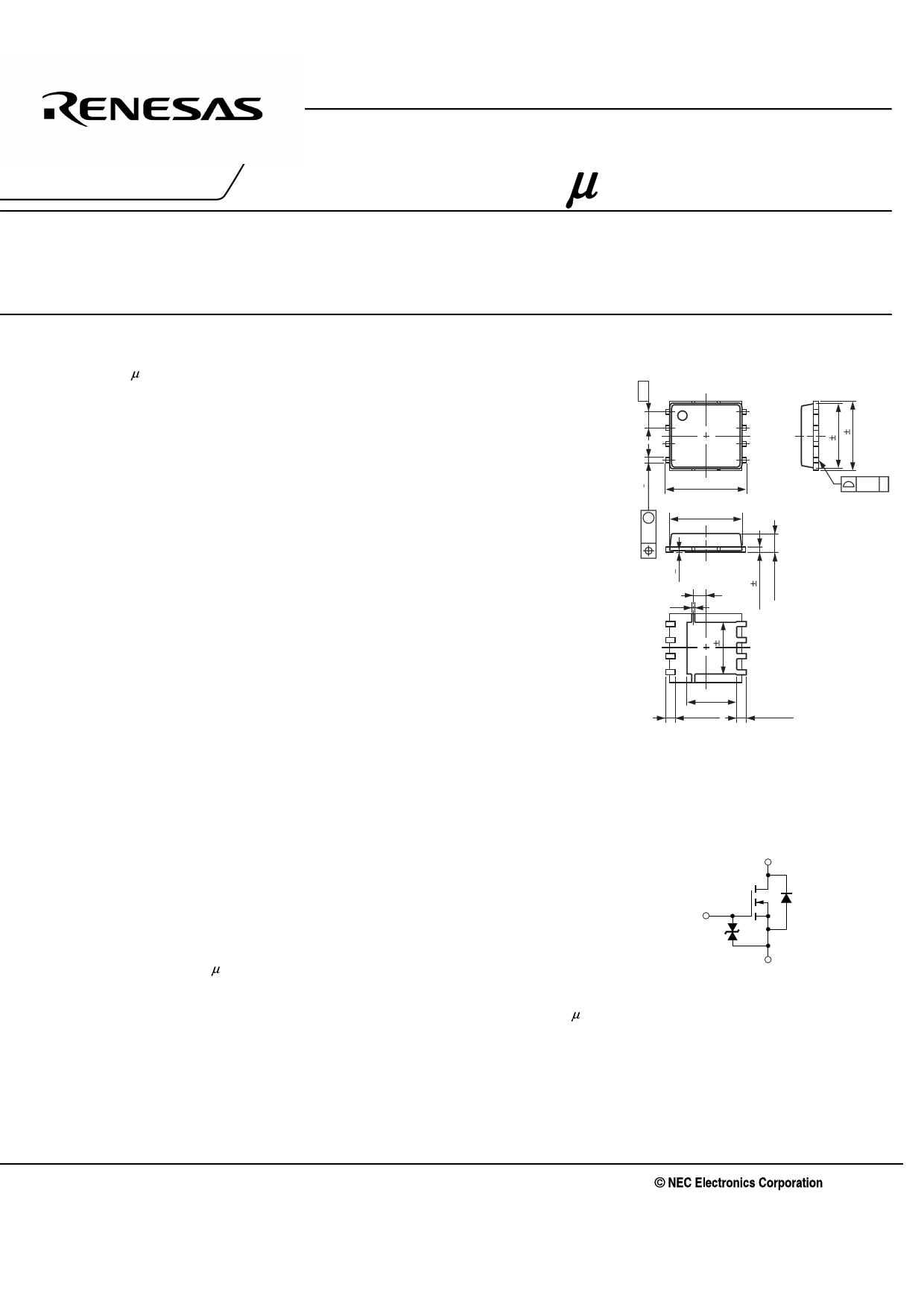
PACKAGE DRAWING (Unit: mm)
1
2
3
4
8
7
6
5
6 ±0.2
5.4 ±0.2
0.10 S
1
0.2
1, 2, 3 : Source
4 : Gate
5, 6, 7, 8: Drain
3.65 ±0.2
0.6 ±0.15
0.7 ±0.15
EQUIVALENT CIRCUIT
Drain
THERMAL RESISTANCE
Channel to Ambient Thermal Resistance Note2
Channel to Case (Drain) Thermal Resistance
Rth(ch-A)
Rth(ch-C)
83.3
1.5
°C/W
°C/W
Notes 1. PW ≤ 10 μs, Duty Cycle ≤ 1%
2. Mounted on a glass epoxy board of 25.4 mm x 25.4 mm x 0.8 mmt
3. Starting Tch = 25°C, VDD = 15 V, RG = 25 Ω, VGS = 20 → 0 V, L = 100 μH
Gate
Body
Diode
Gate
Protection
Diode
Source
Remark The diode connected between the gate and source of the transistor serves as a protector against ESD. When
this device actually used, an additional protection circuit is externally required if a voltage exceeding the rated
voltage may be applied to this device.
The information in this document is subject to change without notice. Before using this document, please
confirm that this is the latest version.
Not all products and/or types are available in every country. Please check with an NEC Electronics
sales representative for availability and additional information.
Document No. G19790EJ1V0DS00 (1st edition)
Date Published May 2009 NS
Printed in Japan
2009
1 page 
μ PA2743T1A
DYNAMIC INPUT CHARACTERISTICS
6
VDD = 24 V
5 15 V
6V
4
3
2
1
ID = 29 A
0
0 10 20 30 40 50
QG - Gate Charge - nC
SOURCE TO DRAIN DIODE FORWARD VOLTAGE
1000
100
VGS = 10 V
10 0 V
1
0.1
0
Pulsed
0.2 0.4 0.6 0.8 1 1.2
VF(S-D) - Source to Drain Voltage - V
ORDERING INFORMATION
PART NUMBER
μ PA2743T1A-E1-AY Note
μ PA2743T1A-E2-AY Note
LEAD PLATING
Pure Sn
PACKING
Tape 3000 p/reel
Note Pb-free (This product does not contain Pb in the external electrode.)
PACKAGE
8-pin HVSON (6051)
0.10 g TYP.
Data Sheet G19790EJ1V0DS
5
5 Page | ||
| Páginas | Total 6 Páginas | |
| PDF Descargar | [ Datasheet UPA2743T1A.PDF ] | |
Hoja de datos destacado
| Número de pieza | Descripción | Fabricantes |
| UPA2743T1A | N-CHANNEL MOS FIELD EFFECT TRANSISTOR | Renesas |
| Número de pieza | Descripción | Fabricantes |
| SLA6805M | High Voltage 3 phase Motor Driver IC. |
Sanken |
| SDC1742 | 12- and 14-Bit Hybrid Synchro / Resolver-to-Digital Converters. |
Analog Devices |
|
DataSheet.es es una pagina web que funciona como un repositorio de manuales o hoja de datos de muchos de los productos más populares, |
| DataSheet.es | 2020 | Privacy Policy | Contacto | Buscar |