|
|
PDF LTC6957-4 Data sheet ( Hoja de datos )
| Número de pieza | LTC6957-4 | |
| Descripción | Dual Output Buffer/Driver/Logic Converter | |
| Fabricantes | Linear | |
| Logotipo |  |
|
Hay una vista previa y un enlace de descarga de LTC6957-4 (archivo pdf) en la parte inferior de esta página. Total 30 Páginas | ||
|
No Preview Available !
Features
n Low Phase Noise Buffer/Driver
n Optimized Conversion of Sine Wave Signals to
Logic Levels
n Three Logic Output Types Available
– LVPECL
– LVDS
– CMOS
n Additive Jitter 45fsRMS (LTC6957-1)
n Frequency Range Up to 300MHz
n 3.15V to 3.45V Supply Operation
n Low Skew 3ps Typical
n Fully Specified from –40°C to 125°C
n 12-Lead MSOP and 3mm × 3mm DFN Packages
Applications
n System Reference Frequency Distribution
n High Speed ADC, DAC, DDS Clock Driver
n Military and Secure Radio
n Low Noise Timing Trigger
n Broadband Wireless Transceiver
n High Speed Data Acquisition
n Medical Imaging
n Test and Measurement
LTC6957-1/LTC6957-2/
LTC6957-3/LTC6957-4
Low Phase Noise, Dual
Output Buffer/Driver/
Logic Converter
Description
The LTC®6957-1/LTC6957-2/LTC6957-3/LTC6957-4 is
a family of very low phase noise, dual output AC signal
buffer/driver/logic level translators. The input signal can
be a sine wave or any logic level (≤2VP-P). There are four
members of the family that differ in their output logic
signal type as follows:
LTC6957-1: LVPECL Logic Outputs
LTC6957-2: LVDS Logic Outputs
LTC6957-3: CMOS Logic, In-Phase Outputs
LTC6957-4: CMOS Logic, Complementary Outputs
The LTC6957 will buffer and distribute any logic signal
with minimal additive noise, however, the part really ex-
cels at translating sine wave signals to logic levels. The
early amplifier stages have selectable lowpass filtering
to minimize the noise while still amplifying the signal to
increase its slew rate. This input stage filtering/noise limit-
ing is especially helpful in delivering the lowest possible
phase noise signal with slow slewing input signals such
as a typical 10MHz sine wave system reference.
L, LT, LTC, LTM, Linear Technology and the Linear logo are registered trademarks of Linear
Technology Corporation. All other trademarks are the property of their respective owners.
Protected by U.S. Patents 7969189 and 8319551.
Typical Application
3.3V
0.1µF
FILTA
OCXO
100MHz
+7dBm
SINE WAVE
10nF
50Ω
10nF
FILTB
IN+
IN–
V+
GND
SD1
OUT1
TO PLL CHIPS
OR SYSTEM
SAMPLING CLOCKS
OUT2
SD2
6957 TA01a
For more information www.linear.com/LTC6957-1
Additive Phase Noise at 100MHz
–140
–145
SINGLE-ENDED SINE WAVE INPUT
AT +7dBm (500mVRMS)
FILTA = FILTB = GND
–150
–155
LTC6957-2 (LVDS)
LTC6957-4 (CMOS)
–160
LTC6957-3
(CMOS)
–165
100
LTC6957-1 (LVPECL)
1k 10k 100k
OFFSET FREQUENCY (Hz)
1M
69571234 TA01b
6957f
1
1 page 
LTC6957-1/LTC6957-2/
LTC6957-3/LTC6957-4
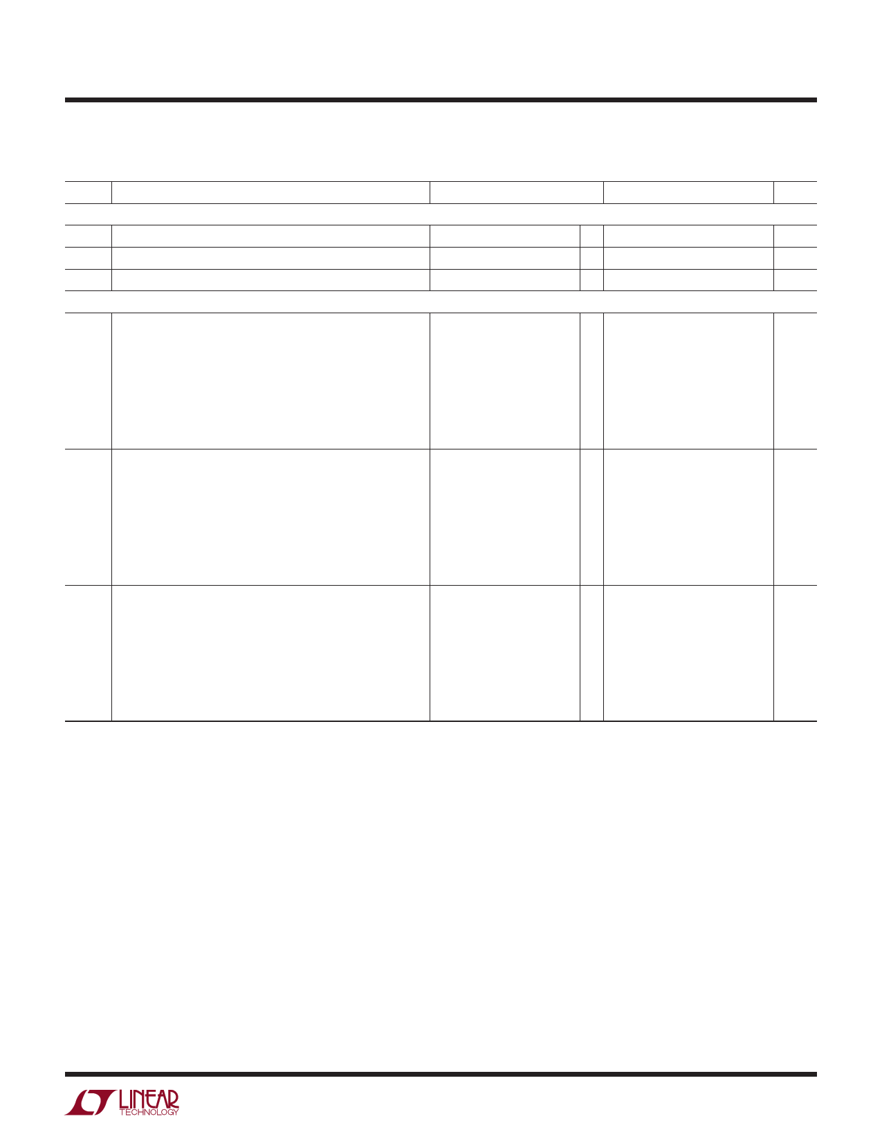
Electrical Characteristics LTC6957-1
The l denotes the specifications which apply over the full operating temperature range, otherwise specifications are at TA = 25°C. V+ = 3.3V,
SD1 = SD2 = 0.4V, FILTA = FILTB = 0.4V, RLOAD = 50Ω connected to 1.3V, unless otherwise specified. All voltages are with respect to ground.
SYMBOL PARAMETER
CONDITIONS
MIN TYP MAX UNITS
Digital Logic Inputs
VIH High Level SD or FILT Input Voltage
VIL Low Level SD or FILT Input Voltage
IIN_DIG Input Current SD or FILT Pins
Additive Phase Noise and Jitter
l V+ – 0.4
l
l
0.1
0.4
±10
V
V
µA
fIN = 300MHz Sine Wave, 7dBm (FILTA = L, FILTB = L)
at 10Hz Offset
at 100Hz Offset
at 1kHz Offset
at 10kHz Offset
at 100kHz Offset
>1MHz Offset
Jitter (10Hz to 150MHz)
Jitter (12kHz to 20MHz)
f IN
=
122.88MHz
Sine Wave, 0dBm (FILTA
at 10Hz Offset
=
H,
FILTB
=
L)
at 100Hz Offset
at 1kHz Offset
at 10kHz Offset
at 100kHz Offset
>1MHz Offset
Jitter (10Hz to 61.44MHz)
Jitter (12kHz to 20MHz)
fIN = 100MHz Sine Wave, 10dBm (FILTA = L, FILTB = L)
at 10Hz Offset
at 100Hz Offset
at 1kHz Offset
at 10kHz Offset
at 100kHz Offset
>1MHz Offset
Jitter (10Hz to 50MHz)
Jitter (12kHz to 20MHz)
–130
–140
–150
–157
–157.5
–157.5
123
45
–137
–146
–154.6
–157
–157.2
–157.2
200
114
–138
–148.1
–156.8
–160.6
–161
–161
142
90
dBc/Hz
dBc/Hz
dBc/Hz
dBc/Hz
dBc/Hz
dBc/Hz
fsRMS
fsRMS
dBc/Hz
dBc/Hz
dBc/Hz
dBc/Hz
dBc/Hz
dBc/Hz
fsRMS
fsRMS
dBc/Hz
dBc/Hz
dBc/Hz
dBc/Hz
dBc/Hz
dBc/Hz
ffssRRMMSS
For more information www.linear.com/LTC6957-1
6957f
5
5 Page 
LTC6957-1/LTC6957-2/
LTC6957-3/LTC6957-4
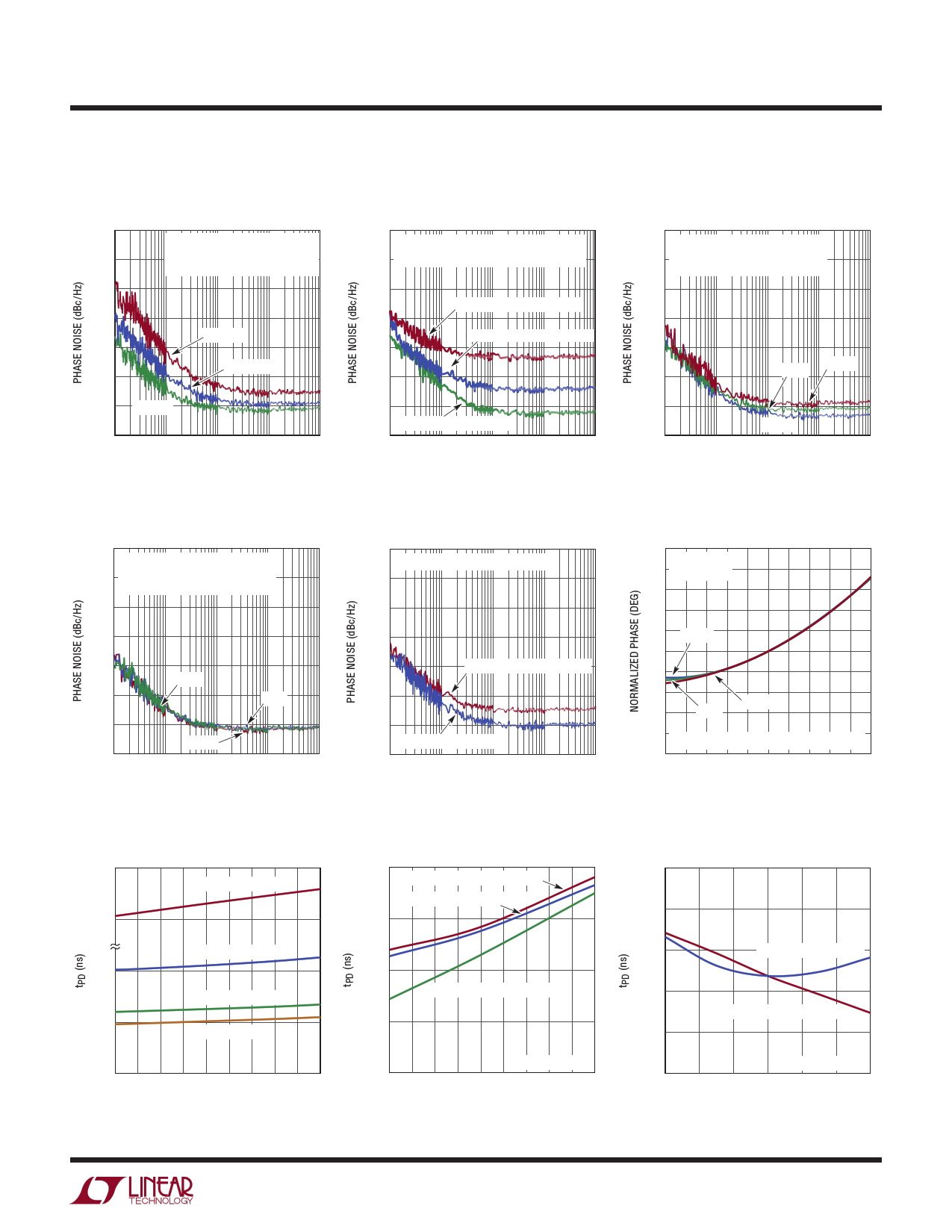
Typical Performance Characteristics LTC6957-1
Additive Phase Noise
vs Input Frequency
–130
–135
SINGLE-ENDED SINE WAVE INPUT
AT 7dBm (500mVRMS)
FILTA = FILTB = L
–140
–145
–150
–155
300MHz
153.6MHz
–160 100MHz
–165
100
1k 10k 100k
OFFSET FREQUENCY (Hz)
1M
69571234 G10
Additive Phase Noise
vs Supply Voltage
–130
–135
SINGLE-ENDED SINE WAVE INPUT,
100MHz at 7dBm (500mVRMS)
FILTA = FILTB = L
–140
–145
–150
–155
–160
–165
100
3.45V
3.3V
3.15V
1k 10k 100k
OFFSET FREQUENCY (Hz)
1M
69571234 G13
tPD vs Temperature
3.5
FILTA = FILTB = H
3.0
FILTA = L, FILTB = H
1.0
FILTA = H, FILTB = L
0.5
FILTA = FILTB = L
0
–55 –35 –15 5 25 45 65 85 105 125
TEMPERATURE (°C)
69571234 G16
Additive Phase Noise
vs Amplitude
–130
–135
SINGLE-ENDED 100MHz SINE WAVE INPUT
SEE APPLICATIONS INFORMATION
–140
–145
–150
–10dBm, FILTA = L, FILTB = H
0dBm, FILTA = H, FILTB = L
–155
–160
+10dBm, FILTA = FILTB = L
–165
100 1k 10k
100k
OFFSET FREQUENCY (Hz)
1M
69571234 G11
Additive Phase Noise at 122.88MHz
–130
–135
SINGLE-ENDED SINE WAVE INPUT
–140
–145
–150
0dBm, FILTA = H, FILTB = L
–155
–160
7dBm, FILTA = FILTB = L
–165
100 1k 10k
100k
OFFSET FREQUENCY (Hz)
1M
69571234 G14
tPD vs Temperature
0.550
V+ = 3.0V, 50Ω LOADS TO 1.3V
V+ = 3.6V, 50Ω LOADS TO 1.9V
0.525
0.500
0.475
V+ = 3.3V, 50Ω LOADS TO 1.3V
FILTA = FILTB = L
0.450
–55 –35 –15 5 25 45 65 85 105 125
TEMPERATURE (°C)
69571234 G17
For more information www.linear.com/LTC6957-1
Additive Phase Noise
vs Temperature
–130
–135
SINGLE-ENDED SINE WAVE INPUT,
100MHz at 7dBm (500mVRMS)
FILTA = FILTB = L
–140
–145
–150
–155
25°C 125°C
–160
–165
100
–55°C
1k 10k 100k
OFFSET FREQUENCY (Hz)
1M
69571234 G12
AM to PM Conversion
5
4
VfIN+
=
=
300MHz
3.3V
3
2
1 –55°C
0
–1
–2
–3
25°C
125°C
–4 EACH CURVE NORMALIZED TO 0° AT 0dBm
–5
–10 –8 –6 –4 –2 0 2 4 6 8 10
INPUT AMPLITUDE (dBm)
69571234 G15
TtPeDrmvsinSautipopnlyVVolotlatgaege and
0.56
0.54
0.52 50Ω LOADS TO V+ –2V
0.50
0.48
0.46
3
50Ω LOADS TO FIXED 1.3V
FILTA = FILTB = L
3.1 3.2 3.3 3.4 3.5
SUPPLY VOLTAGE (V)
3.6
69571234 G18
6957f
11
11 Page | ||
| Páginas | Total 30 Páginas | |
| PDF Descargar | [ Datasheet LTC6957-4.PDF ] | |
Hoja de datos destacado
| Número de pieza | Descripción | Fabricantes |
| LTC6957-1 | Dual Output Buffer/Driver/Logic Converter | Linear |
| LTC6957-2 | Dual Output Buffer/Driver/Logic Converter | Linear |
| LTC6957-3 | Dual Output Buffer/Driver/Logic Converter | Linear |
| LTC6957-4 | Dual Output Buffer/Driver/Logic Converter | Linear |
| Número de pieza | Descripción | Fabricantes |
| SLA6805M | High Voltage 3 phase Motor Driver IC. |
Sanken |
| SDC1742 | 12- and 14-Bit Hybrid Synchro / Resolver-to-Digital Converters. |
Analog Devices |
|
DataSheet.es es una pagina web que funciona como un repositorio de manuales o hoja de datos de muchos de los productos más populares, |
| DataSheet.es | 2020 | Privacy Policy | Contacto | Buscar |
