|
|
|
PDF JTS3702 Data sheet ( Hoja de datos )
| Número de pieza | JTS3702 | |
| Descripción | Micropower dual CMOS voltage comparator | |
| Fabricantes | STMicroelectronics | |
| Logotipo | ||
Hay una vista previa y un enlace de descarga de JTS3702 (archivo pdf) en la parte inferior de esta página. Total 10 Páginas | ||
|
No Preview Available !
JTS3702
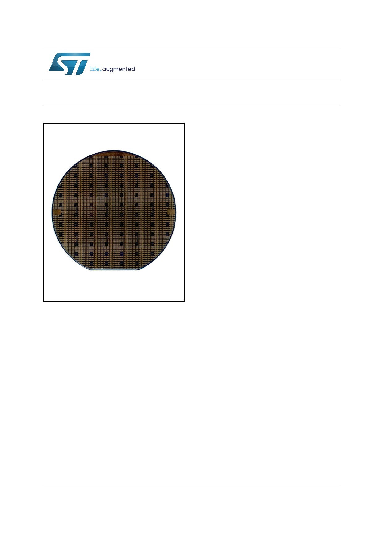
Micropower dual CMOS voltage comparator: unsawn wafer
Datasheet - production data
Related products
• See TS3702 for plastic packaged version
Description
The JTS3702 is a micro power CMOS dual
voltage comparator with an extremely low
consumption of 9 µA typical per comparator (20
times less than the bipolar LM393). The push-pull
CMOS output stage allows power and space
saving by eliminating the external pull-up resistor
required by usual open-collector output
comparators. Thus, response times remain
similar to the LM393.
Unsawn wafer
Features
• Push-pull CMOS output (no external pull-up
resistor required)
• Extremely low supply current: 9 µA typ per
comparator
• Wide single supply range: 2.7 V to 16 V or dual
supplies (±1.35 V to ±8 V)
• Extremely low input bias current: 1 pA typ
• Extremely low input offset current: 1 pA typ
• Input common-mode voltage range includes
GND
• High input impedance: 1012 Ω typ
• Fast response time: 2 µs typ for 5 mV overdrive
• Functionally compatible with bipolar LM393
December 2013
This is information on a product in full production.
DocID025632 Rev 1
1/10
www.st.com
1 page 
JTS3702
Absolute maximum ratings and operating conditions
2 Absolute maximum ratings and operating conditions
Table 2. Absolute maximum ratings (AMR)
Symbol
VCC+
Vid
Vi
Vo
Io
IF
Tstg
ESD
Parameter
Supply voltage(1)
Differential input voltage(2)
Input voltage(3)
Output voltage
Output current
Forward current in ESD protection diodes on Input(4)
Storage temperature range
HBM: human body model(5)
MM: machine model(6)
Value
18
±18
18
18
20
50
-65 to +150
400
50
Unit
V
mA
°C
V
1. All voltage values, except differential voltage, are with respect to network ground terminal.
2. Differential voltages are the non-inverting input terminal with respect to the inverting input terminal.
3. The magnitude of the input and the output voltages must never exceed the magnitude of the positive and
negative supply voltages.
4. Guaranteed by design.
5.
Human body
all couples of
mpiondceol:m1b0i0naptFiodnisscwhitahrgoethdetrhproinusghfloaa1tin.5g.kΩ
resistor
between
two
pins
of
the
device,
done
for
6. Machine model: a 200 pF cap is charged to the specified voltage, then discharged directly between two
pins of the device
combinations with
with no external series
other pins floating.
resistor
(internal
resistor
<
5
Ω),
done
for
all
couples
of
pin
Symbol
VCC+
Vicm
Toper
Table 3. Operating conditions
Parameter
Supply voltage
Common mode input voltage range
Tmin. ≤Tamb ≤Tmax
Operating free-air temperature range - JTS3702C
Value
2.7 to 16
0
0
to
to
VVCCCC++
-1.2
-1.5
0 to +70
Unit
V
°C
DocID025632 Rev 1
5/10
10
5 Page | ||
| Páginas | Total 10 Páginas | |
| PDF Descargar | [ Datasheet JTS3702.PDF ] | |
Hoja de datos destacado
| Número de pieza | Descripción | Fabricantes |
| JTS3702 | Micropower dual CMOS voltage comparator | STMicroelectronics |
| Número de pieza | Descripción | Fabricantes |
| SLA6805M | High Voltage 3 phase Motor Driver IC. |
Sanken |
| SDC1742 | 12- and 14-Bit Hybrid Synchro / Resolver-to-Digital Converters. |
Analog Devices |
|
DataSheet.es es una pagina web que funciona como un repositorio de manuales o hoja de datos de muchos de los productos más populares, |
| DataSheet.es | 2020 | Privacy Policy | Contacto | Buscar |