|
|
|
PDF CHT4690-QAG Data sheet ( Hoja de datos )
| Número de pieza | CHT4690-QAG | |
| Descripción | GaAs Monolithic Microwave IC | |
| Fabricantes | United Monolithic Semiconductors | |
| Logotipo | ||
Hay una vista previa y un enlace de descarga de CHT4690-QAG (archivo pdf) en la parte inferior de esta página. Total 14 Páginas | ||
|
No Preview Available !
CHT4690-QAG
RoHS COMPLIANT
5-30GHz ATTENUATOR
GaAs Monolithic Microwave IC in SMD leadless package
Description
The CHT4690-QAG is a variable 5-30GHz
attenuator designed for a wide range of
applications, from military to commercial
communication systems.
The circuit is manufactured with a
MESFET process, 0.7µm gate length, via
holes through the substrate and air
bridges.
It is supplied in lead-free package.
Main Features
■ Broadband performance: 5-30GHz
■ 25dBm typical input 1dB compression
point (Any attenuation)
■ 30dB dynamic range
■ DC bias: -5V<V1<0V ; -5V<V2<0V
■ Package type: 16Leads QFN3x3
Attenuation versus frequency & V1, V2
Main Characteristics
Temp. = 25°C
Symbol
Parameter
Min Typ Max Unit
Fin Input frequency range
5 30 GHz
Min Att. |S21| (V1=-5V;V2=-5V) (10 to 24GHz)
4 dB
Max Att. |S21| (V1=0V;V2=0V) (10 to 30GHz)
35 dB
Pin1dB Input 1dB compression point (any
attenuation)
25
dBm
ESD Protection: Electrostatic discharge sensitive device. Observe handling precautions!
Ref. : CHT4690QAG0211 - 30 Jul 2010
1/14
Specifications subject to change without notice
United Monolithic Semiconductors S.A.S.
Route Départementale 128 - BP46 - 91401 Orsay Cedex France
Tel.: +33 (0) 1 69 33 03 08 - Fax: +33 (0) 1 69 33 03 09
1 page 
5-30GHz Attenuator
CHT4690-QAG
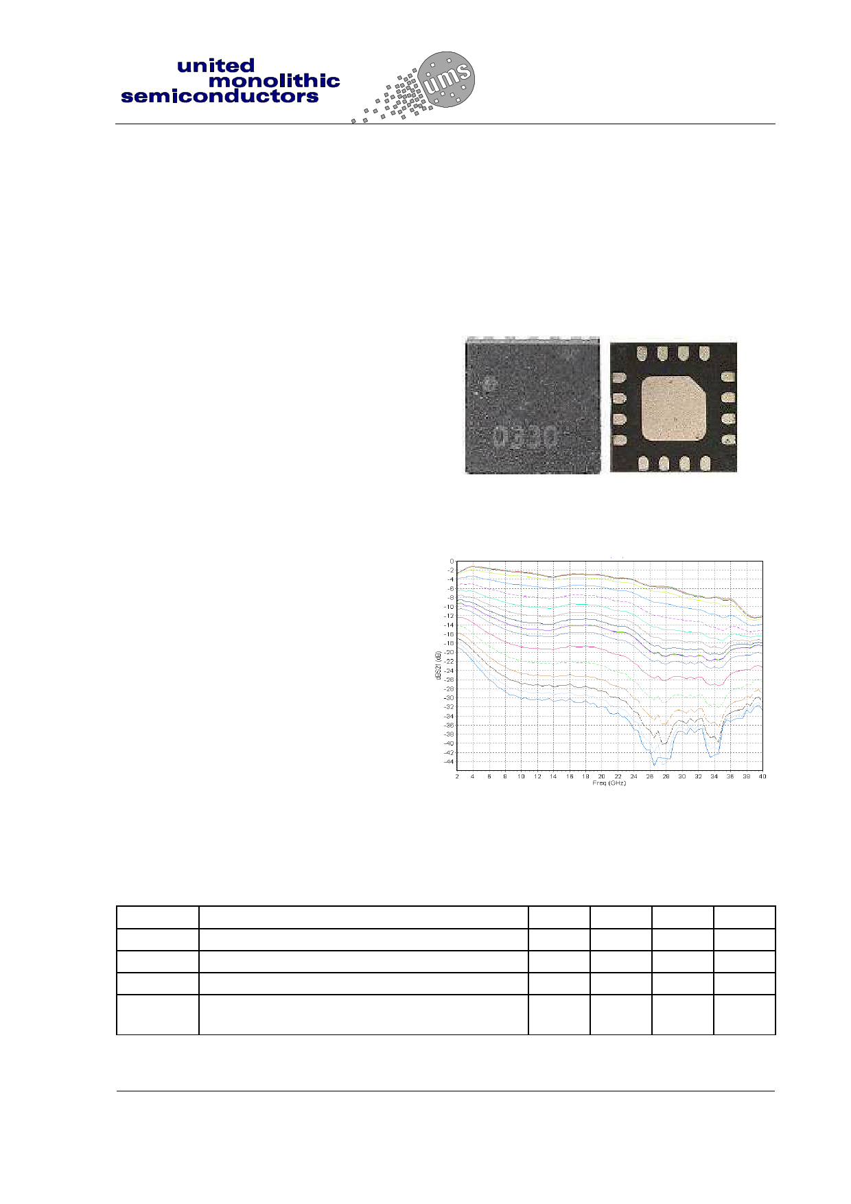
Typical Results
Temp. = +25°C
Measurements performed in the package access, using the proposed land pattern & board
96272.
Attenuation versus frequency
V1 = -5V to 0V & V2= -5V and after V1= 0V & V2 = -5V to 0V
Ref. : CHT4690QAG0211 - 30 Jul 2010
5/14
Specifications subject to change without notice
Route Départementale 128, BP46 - 91401 ORSAY Cedex - FRANCE
Tel.: +33 (0) 1 69 33 03 08 - Fax: +33 (0) 1 69 33 03 09
5 Page 
5-30GHz Attenuator
CHT4690-QAG
Definition of the Sij reference planes
The reference planes are defined from the
footprint of the recommended
characterization board 95542 shown below.
The reference is the symmetrical axis of the
package. The input and output reference
planes are located at 2.65mm offset (input
wise and output wise respec.) from this axis.
Then, the given Sij incorporates this land
pattern.
2.65 2.65
Application note
The design of the motherboard has a strong impact on the over all performance since the
transition from the motherboard to the package is comparably large. In case of the SMD type
packages of United Monolithic Semiconductors the motherboard should be designed
according to the information given in the following to achieve good performance. Other
configurations are also possible but can lead to different results. If you need advise please
contact United Monolithic Semiconductors for further information.
SMD type packages of UMS should allow design and fabrication of micro- and mm-wave
modules at low cost. Therefore, a suitable motherboard environment has been chosen. All
tests and verifications have been performed on Rogers RO4003. This material exhibits a
permittivity of 3.38 and has been used with a thickness of 200µm [8 mils] and a 1/2oz or less
copper cladding. The corresponding 50Ohm transmission line has a strip width of about
460µm [approx. 18 mils].
The contact areas on the motherboard for the package connections should be designed
according to the footprint given below. The proper via structure under the ground pad is very
important in order to achieve a good RF and lifetime performance. All tests have been done
by using a grid of plated through vias with a diameter of less than 300µm [12 mils] and a
spacing of less than 700µm [28 mils] from the centres of two adjacent vias. The via grid
should cover the whole space under the ground pad and the vias closest to the RF ports
should be located near the edge of the pad to allow a good RF ground connection. Since the
vias are important for heat transfer, a proper via filling should be guaranteed during the
mounting procedure to get a low thermal resistance between package and heat sink. For
power devices the use of heat slugs in the motherboard instead of a grid of via’s is
recommended.
For the mounting process the SMD type package can be handled as a standard surface
mount component. The use of either solder or conductive epoxy is possible. The solder
thickness after reflow should be typical 50µm [2 mils] and the lateral alignment between the
package and the motherboard should be within 50µm [2 mils]. Caution should be taken to
obtain a good and reliable contact over the whole pad areas. Voids or other improper
connections, in particular, between the ground pads of motherboard and package will lead to
a deterioration of the RF performance and the heat dissipation. The latter effect can reduce
drastically reliability and lifetime of the product.
Ref. : CHT4690QAG0211 - 30 Jul 2010
11/14
Specifications subject to change without notice
Route Départementale 128, BP46 - 91401 ORSAY Cedex - FRANCE
Tel.: +33 (0) 1 69 33 03 08 - Fax: +33 (0) 1 69 33 03 09
11 Page | ||
| Páginas | Total 14 Páginas | |
| PDF Descargar | [ Datasheet CHT4690-QAG.PDF ] | |
Hoja de datos destacado
| Número de pieza | Descripción | Fabricantes |
| CHT4690-QAG | GaAs Monolithic Microwave IC | United Monolithic Semiconductors |
| Número de pieza | Descripción | Fabricantes |
| SLA6805M | High Voltage 3 phase Motor Driver IC. |
Sanken |
| SDC1742 | 12- and 14-Bit Hybrid Synchro / Resolver-to-Digital Converters. |
Analog Devices |
|
DataSheet.es es una pagina web que funciona como un repositorio de manuales o hoja de datos de muchos de los productos más populares, |
| DataSheet.es | 2020 | Privacy Policy | Contacto | Buscar |