|
|
|
PDF NDD03N40Z Data sheet ( Hoja de datos )
| Número de pieza | NDD03N40Z | |
| Descripción | N-Channel Power MOSFET / Transistor | |
| Fabricantes | ON Semiconductor | |
| Logotipo | ||
Hay una vista previa y un enlace de descarga de NDD03N40Z (archivo pdf) en la parte inferior de esta página. Total 9 Páginas | ||
|
No Preview Available !
NDD03N40Z, NDT03N40Z
N-Channel Power MOSFET
400 V, 3.4 W
Features
• 100% Avalanche Tested
• Extremely High dv/dt Capability
• Gate Charge Minimized
• Very Low Intrinsic Capacitance
• Improved Diode Reverse Recovery Characteristics
• Zener−protected
• These Devices are Pb-Free, Halogen Free/BFR Free and are RoHS
Compliant
ABSOLUTE MAXIMUM RATINGS (TJ = 25°C unless otherwise noted)
Parameter
Symbol NDD NDT Unit
Drain−to−Source Voltage
Gate−to−Source Voltage
Continuous Drain Current
Steady State, TC = 25°C (Note 1)
VDSS
VGS
ID
400
±30
2.1 0.5
V
V
A
Continuous Drain Current
Steady State, TC = 100°C (Note 1)
ID 1.3 0.3 A
Power Dissipation
Steady State, TC = 25°C
PD 37 2.0 W
Pulsed Drain Current
Continuous Source Current (Body
Diode)
IDM 8.0 7.2 A
IS 2.1 0.5 A
Single Pulse Drain−to−Source
Avalanche Energy (ID = 1 A)
Peak Diode Recovery (Note 2)
Maximum Temperature for Soldering
Leads
EAS
dV/dt
TL
42 mJ
12 V/ns
260 °C
Operating Junction and Storage
Temperature
TJ, TSTG −55 to +150 °C
Stresses exceeding those listed in the Maximum Ratings table may damage the
device. If any of these limits are exceeded, device functionality should not be
assumed, damage may occur and reliability may be affected.
1. Limited by maximum junction temperature
2. IS ≤ 2.4 A, di/dt ≤ 400 A/ms, VDD ≤ BVDSS, TJ = +150°C
THERMAL RESISTANCE
Parameter
Symbol Value Unit
Junction−to−Case (Drain)
NDD03N40Z
Junction−to−Ambient Steady State
NDD03N40Z (Note 4)
NDD03N40Z−1 (Note 3)
NDT03N40Z (Note 4)
NDT03N40Z (Note 5)
RqJC
RqJA
3.4 °C/W
°C/W
42
96
62
149
3. Insertion mounted
4. Surface mounted on FR4 board using 1″ sq. pad size
(Cu area = 1.127″ sq. [2 oz] including traces)
5. Surface−mounted on FR4 board using minimum recommended pad size
(Cu area = 0.026” sq. [2 oz]).
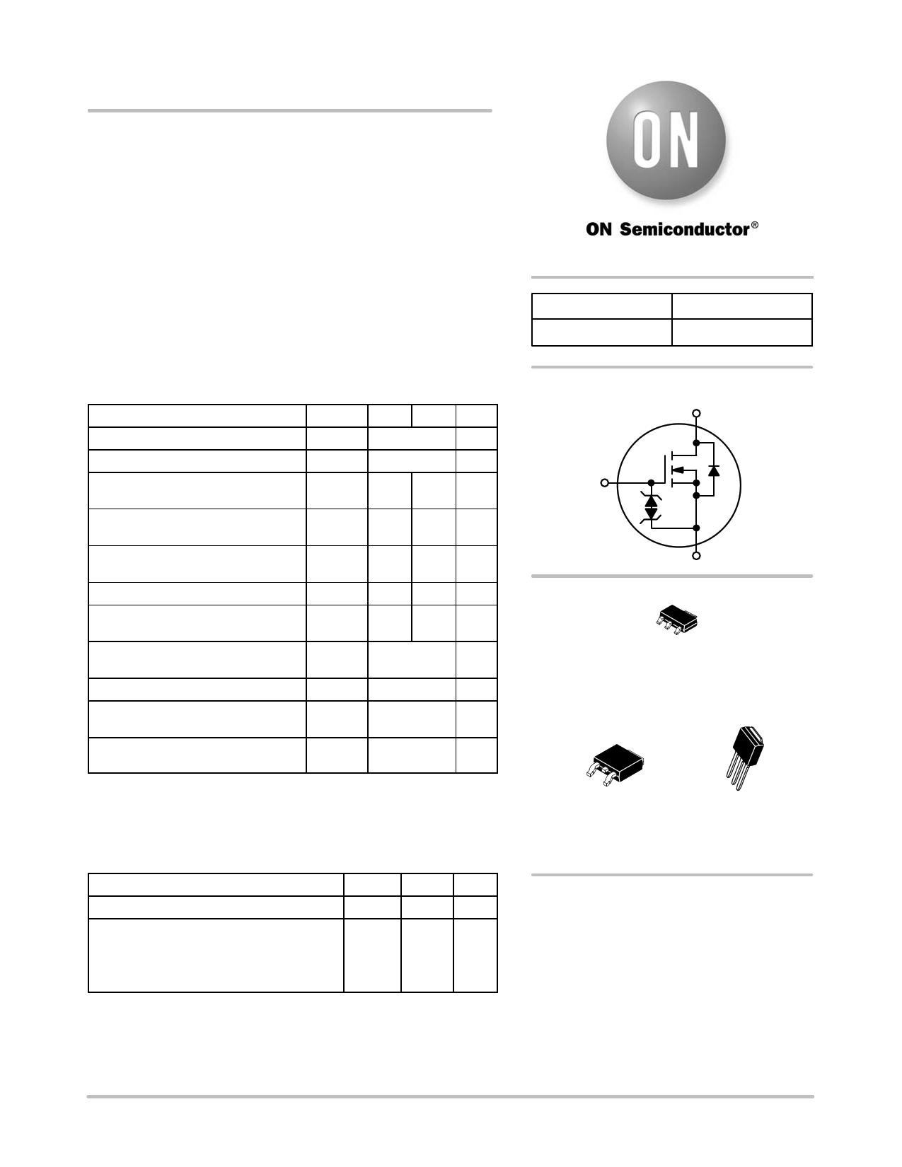
http://onsemi.com
V(BR)DSS
400 V
RDS(ON) MAX
3.4 W @ 10 V
N−Channel
D (2, 4)
G (1)
S (3)
4
1 23
SOT−223
CASE 318E
STYLE 3
4
4
12
3
DPAK
CASE 369C
STYLE 2
1 23
IPAK
CASE 369D
STYLE 2
MARKING & ORDERING INFORMATION
See detailed ordering, marking and shipping information in the
package dimensions section on page 3 of this data sheet.
© Semiconductor Components Industries, LLC, 2014
May, 2014 − Rev. 1
1
Publication Order Number:
NDD03N40Z/D
1 page 
NDD03N40Z, NDT03N40Z
TYPICAL CHARACTERISTICS
1.15
1.10
1.05
ID = 50 mA
1.00
0.95
0.90
0.85
0.80
0.75
0.70
0.65
−50 −25 0 25 50 75 100 125 150
TJ, JUNCTION TEMPERATURE (°C)
Figure 7. Threshold Voltage Variation with
Temperature
10,000
1000
TJ = 150°C
100 TJ = 125°C
10 TJ = 100°C
1
0 50 100 150 200 250 300 350 400
VDS, DRAIN−TO−SOURCE VOLTAGE (V)
Figure 8. Drain−to−Source Leakage Current
vs. Voltage
1000
COSS
CISS
100 CRSS
10
1
0.1
1
VGS = 0 V
TJ = 25°C
f = 1 MHz
12
11
10
9
8
7
6
5
4
3
2
1
0
10 100 1000 0
VDS, DRAIN−TO−SOURCE VOLTAGE (V)
Figure 9. Capacitance Variation
VDS
QGS
QT
QGD
250
200
VGS
150
100
VDS = 200 V
TJ = 25°C
ID = 2.4 A
50
0
12 3 4567
QG, TOTAL GATE CHARGE (nC)
Figure 10. Gate−to−Source and
Drain−to−Source Voltage vs. Total Charge
100
VGS = 10 V
VDD = 200 V
ID = 2.4 A
10
td(off)
tr
tf
td(on)
10
TJ = 100°C
1 TJ = 125°C
0.1
TJ = 150°C
TJ = 25°C
0.01
1
0.1
1
10 100
RG, GATE RESISTANCE (W)
Figure 11. Resistive Switching Time Variation
vs. Gate Resistance
0.001
TJ = −55°C
0.2 0.3 0.4 0.5 0.6 0.7 0.8 0.9 1.0 1.1 1.2
VSD, SOURCE−TO−DRAIN VOLTAGE (V)
Figure 12. Diode Forward Voltage vs. Current
http://onsemi.com
5
5 Page | ||
| Páginas | Total 9 Páginas | |
| PDF Descargar | [ Datasheet NDD03N40Z.PDF ] | |
Hoja de datos destacado
| Número de pieza | Descripción | Fabricantes |
| NDD03N40Z | N-Channel Power MOSFET / Transistor | ON Semiconductor |
| Número de pieza | Descripción | Fabricantes |
| SLA6805M | High Voltage 3 phase Motor Driver IC. |
Sanken |
| SDC1742 | 12- and 14-Bit Hybrid Synchro / Resolver-to-Digital Converters. |
Analog Devices |
|
DataSheet.es es una pagina web que funciona como un repositorio de manuales o hoja de datos de muchos de los productos más populares, |
| DataSheet.es | 2020 | Privacy Policy | Contacto | Buscar |