|
|
|
PDF NCP4688 Data sheet ( Hoja de datos )
| Número de pieza | NCP4688 | |
| Descripción | Low Noise LDO Linear Voltage Regulator | |
| Fabricantes | ON Semiconductor | |
| Logotipo | ||
Hay una vista previa y un enlace de descarga de NCP4688 (archivo pdf) en la parte inferior de esta página. Total 14 Páginas | ||
|
No Preview Available !
NCP4688
150 mA, Low Noise, LDO
Linear Voltage Regulator
The NCP4688 is a CMOS 150 mA LDO linear voltage regulator
with high output voltage accuracy which features a low noise output
voltage and high ripple rejection. The low level of output noise
10 mVrms typically is kept at any output voltage. The very common
SOT23−5 package and small mDFN 1x1 package are suitable for
industrial applications, portable communication equipments and RF
modules.
Features
• Operating Input Voltage Range: 2 V to 5.25 V
• Output Voltage Range: 1.2 to 4.8 V (available in 0.1 V steps)
• ±1% Output Voltage Accuracy
• Output Noise: 10 mVrms
• Line Regulation: 0.02%/V
• Current Limit Circuit
• High PSRR: 80 dB at 1 kHz, 75 dB at 10 kHz
• Available in SOT−23−5 and mDFN 1.0 x 1.0 mm Package
• These are Pb−Free Devices
Typical Applications
• Home Appliances, Industrial Equipment
• Cable Boxes, Satellite Receivers, Entertainment Systems
• Car Audio Equipment, Navigation Systems
• Notebook Adaptors, LCD TVs, Cordless Phones and Private LAN
Systems
• RF Modules
VIN NCP4688x
VOUT
VIN VOUT
C1
1.0 mF
CE
GND
C2
1.0 mF
http://onsemi.com
MARKING
DIAGRAMS
SOT−23−5
CASE 1212
XXXMM
1
1
UDFN−4
CASE 517BR
XX
MG
1G
(Top Views)
XX, XXX = Specific Device Code
M, MM = Date Code
G = Pb−Free Package
(*Note: Microdot may be in either location)
ORDERING INFORMATION
See detailed ordering and shipping information in the package
dimensions section on page 12 of this data sheet.
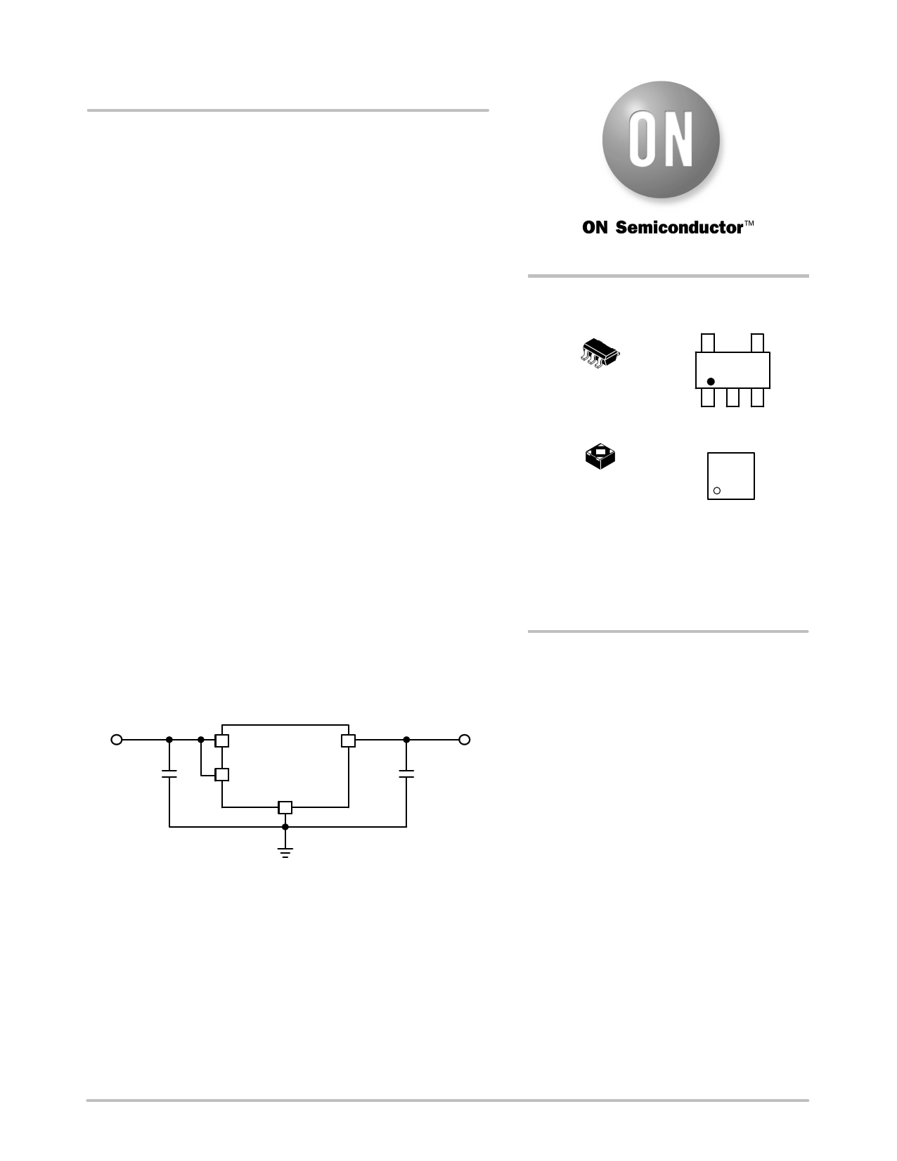
Figure 1. Typical Application Schematic
© Semiconductor Components Industries, LLC, 2012
February, 2012 − Rev. 1
1
Publication Order Number:
NCP4688/D
1 page 
NCP4688
TYPICAL CHARACTERISTICS
80
70
60
50
40
30
20
10
0
01 2 3 4 5
INPUT VOLTAGE (V)
Figure 9. Supply Current vs. Input Voltage
NCP4688xx12
6
90
80
70
60
50
40
30
20
10
0
012 3 45 6
INPUT VOLTAGE (V)
Figure 10. Supply Current vs. Input Voltage
NCP4688xx25
90
80
70
60
50
40
30
20
10
0
012 3 45 6
INPUT VOLTAGE (V)
Figure 11. Supply Current vs. Input Voltage
NCP4688xx40
80
75
70
65
60
55
50
−50 −25 0 25 50 75 100
TEMPERATURE (°C)
Figure 12. Supply Current vs. Temperature
NCP4688xx12
80 80
75 75
70 70
65 65
60 60
55
50
−50
−25
0
25 50 75 100
TEMPERATURE (°C)
Figure 13. Supply Current vs. Temperature
NCP4688xx25
55
50
−50 −25 0 25 50 75 100
TEMPERATURE (°C)
Figure 14. Supply Current vs. Temperature
NCP4688xx40
http://onsemi.com
5
5 Page 
NCP4688
APPLICATION INFORMATION
A typical application circuit for NCP4688 series is shown
in the Figure 41.
VIN
C1
1.0 mF
NCP4688x
VIN VOUT
CE
GND
VOUT
C2
1.0 mF
Figure 41. Typical Application Schematic
Input Decoupling Capacitor (C1)
A 1.0 mF ceramic input decoupling capacitor should be
connected as close as possible to the input and ground pin of
the NCP4688 device. Higher values and lower ESR
improves line transient response.
Output Decoupling Capacitor (C2)
A 1.0 mF ceramic output decoupling capacitor is sufficient
to achieve stable operation of the device. If tantalum
capacitor is used, and its ESR is high, the loop oscillation
may result. For information about ESR see Figures 42, 43
and 44. The capacitor should be connected as close as
possible to the output and ground pin. Larger values and
lower ESR improves dynamic parameters.
Enable Operation
The enable pin CE may be used for turning the regulator
on and off. The IC is switched on when a high level voltage
is applied to the CE pin. The enable pin has an internal pull
down current source which assure off state of LDO in case
the CE pin will stay floating. If the enable function is not
needed connect CE pin to VIN.
The D version of the NCP4688 device includes a
transistor between VOUT and GND that is used for faster
discharging of the output capacitor. This function is
activated when the IC goes into disable mode.
Thermal Consideration
As a power across the IC increase, it might become
necessary to provide some thermal relief. The maximum
power dissipation supported by the device is dependent
upon board design and layout. Mounting pad configuration
on the PCB, the board material, and also the ambient
temperature affect the rate of temperature increase for the
part. When the device has good thermal conductivity
through the PCB the junction temperature will be relatively
low in high power dissipation applications.
ESR vs. Output Current
When using the NCP4688 devices, consider the following
points:
The relation between Output Current Iout and ESR of the
output capacitor are shown below in Figures 42, 43 and 44.
The conditions when the device performs stable operation
are marked as the hatched area in the charts.
100 100
10 10
11
0.1 0.1
0.01
0
25 50
75 100 125 150
LOAD CURRENT (mA)
Figure 42. ESR vs. Load Current NCP4688xx12
0.01
0
25 50 75 100 125 150
LOAD CURRENT (mA)
Figure 43. ESR vs. Load Current NCP4688xx25
http://onsemi.com
11
11 Page | ||
| Páginas | Total 14 Páginas | |
| PDF Descargar | [ Datasheet NCP4688.PDF ] | |
Hoja de datos destacado
| Número de pieza | Descripción | Fabricantes |
| NCP4680 | Low Noise Low Dropout Regulator | ON Semiconductor |
| NCP4681 | (NCP4681 / NCP4684) Low Dropout Regulator | ON Semiconductor |
| NCP4682 | (NCP4682 / NCP4685) Low Dropout Regulator | ON Semiconductor |
| NCP4683 | Low Dropout Regulator | ON Semiconductor |
| Número de pieza | Descripción | Fabricantes |
| SLA6805M | High Voltage 3 phase Motor Driver IC. |
Sanken |
| SDC1742 | 12- and 14-Bit Hybrid Synchro / Resolver-to-Digital Converters. |
Analog Devices |
|
DataSheet.es es una pagina web que funciona como un repositorio de manuales o hoja de datos de muchos de los productos más populares, |
| DataSheet.es | 2020 | Privacy Policy | Contacto | Buscar |