|
|
|
PDF GS1661A Data sheet ( Hoja de datos )
| Número de pieza | GS1661A | |
| Descripción | HD/SD SDI Receiver | |
| Fabricantes | Semtech | |
| Logotipo | ||
Hay una vista previa y un enlace de descarga de GS1661A (archivo pdf) en la parte inferior de esta página. Total 30 Páginas | ||
|
No Preview Available !
GS1661A
HD/SD SDI Receiver, with Integrated Adaptive Cable Equalizer complete with
SMPTE Video Processing
Key Features
• Operation at 1.485Gb/s, 1.485/1.001Gb/s and 270Mb/s
• Supports SMPTE 292M, SMPTE 259M-C and DVB-ASI
• Integrated adaptive cable equalizer
• Typical equalized length of Belden 1694A cable:
230m at 1.485Gb/s
440m at 270Mb/s
• Integrated Reclocker with low phase noise, integrated
VCO
• Serial digital reclocked, or non-reclocked output
• Ancillary data extraction
• Parallel data bus selectable as either 20-bit or 10-bit
• Comprehensive error detection and correction
features
• Output H, V, F or CEA 861 Timing Signals
• 1.2V digital core power supply, 1.2V and 3.3V analog
power supplies, and selectable 1.8V or 3.3V I/O power
supply
• GSPI Host Interface
• Wide temperature range of -40ºC to +85ºC
• Low power operation (typically 460mW)
• Small 11mm x 11mm 100-ball BGA package
• Pb-free and RoHS compliant
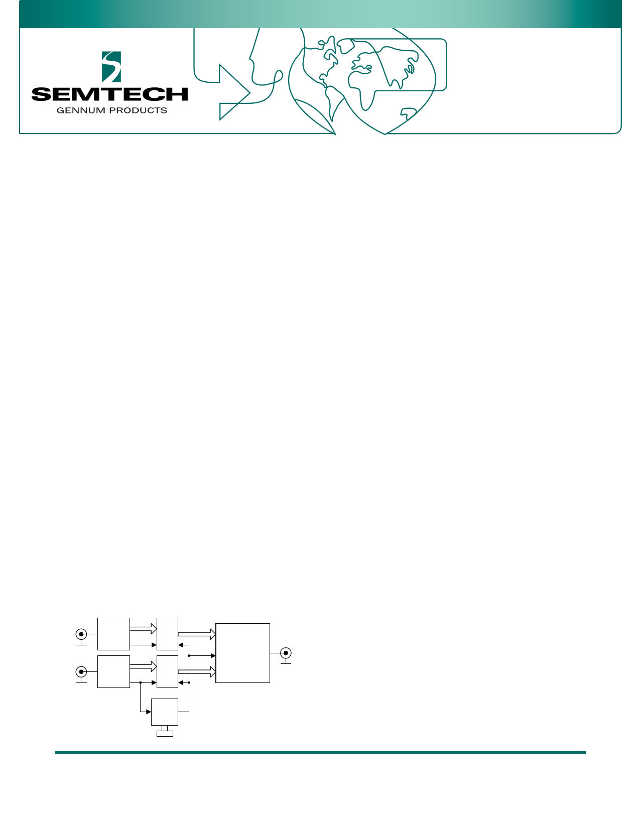
Applications
HD-SDI
Link A
HD-SDI
Link B
Application: Dual Link (HD-SDI)
to Single Link (3G-SDI) Converter
HD-SDI
Deserializer
GS1661A
10-bit
HV F/PCLK
FIFO
WR
HD-SDI
Deserializer
GS1661A
10-bit
HV F/PCLK
FIFO
WR
10-bit
HV F/PCLK
10-bit
GS2962
3G-SDI
GS4910
HVF
X TAL
Description
The GS1661A is a multi-rate SDI integrated Receiver which
includes complete SMPTE processing, as per SMPTE 292M
and SMPTE 259M-C. The SMPTE processing features can be
bypassed to support signals with other coding schemes.
The GS1661A integrates Gennum's adaptive cable
equalizer technology, achieving unprecedented cable
lengths and jitter tolerance. It features DC restoration to
compensate for the DC content of SMPTE pathological
signals.
The device features an Integrated Reclocker with an
internal VCO and a wide Input Jitter Tolerance (IJT) of
0.7UI.
A serial digital loop-through output is provided, which can
be configured to output either reclocked or non-reclocked
serial digital data. The serial digital output can be
connected to an external cable driver.
The device operates in one of four basic modes: SMPTE
mode, DVB-ASI mode, Data-Through mode or Standby
mode.
In SMPTE mode (the default operating mode), the GS1661A
performs full SMPTE processing, and features a number of
data integrity checks and measurement capabilities.
The device also supports ancillary data extraction, and can
provide entire ancillary data packets through
host-accessible registers. It also provides a variety of other
packet detection and error handling features. All of these
processing features are optional, and may be individually
enabled or disabled through register programming.
In DVB-ASI mode, sync word detection, alignment and
8b/10b decoding is applied to the received data stream.
In Data-Through mode all forms of SMPTE and DVB-ASI
processing are disabled, and the device can be used as a
simple serial to parallel converter.
The device can also operate in a lower power Standby
mode. In this mode, no signal processing is carried out and
the parallel output is held static.
GS1661A HD/SD SDI Receiver
Data Sheet
54387 - 2
September 2012
www.semtech.com
1 of 85
1 page 
List of Figures
Figure 3-1: Digital Input Pin with Schmitt Trigger............................................................................... 20
Figure 3-2: Bidirectional Digital Input/Output Pin.............................................................................. 20
Figure 3-3: Bidirectional Digital Input/Output Pin with programmable drive strength......... 21
Figure 3-4: XTAL1/XTAL2/XTAL-OUT ................................................................................................... 21
Figure 3-5: VBG .............................................................................................................................................. 22
Figure 3-6: LB_CONT .................................................................................................................................... 22
Figure 3-7: Loop Filter .................................................................................................................................. 22
Figure 3-8: SDO/SDO .................................................................................................................................... 23
Figure 3-9: Equalizer Input Equivalent Circuit .................................................................................... 23
Figure 4-1: GS1661A Integrated EQ Block Diagram .......................................................................... 25
Figure 4-2: 27MHz Clock Sources ............................................................................................................ 28
Figure 4-3: PCLK to Data and Control Signal Output Timing - SDR Mode 1 .............................. 31
Figure 4-4: PCLK to Data and Control Signal Output Timing - SDR Mode 2 .............................. 32
Figure 4-5: Switch Line Locking on a Non-Standard Switch Line ................................................. 36
Figure 4-6: H:V:F Output Timing - HDTV 20-bit Mode ..................................................................... 39
Figure 4-7: H:V:F Output Timing - HDTV 10-bit Mode ..................................................................... 39
Figure 4-8: H:V:F Output Timing - HD 20-bit Output Mode ............................................................ 40
Figure 4-9: H:V:F Output Timing - HD 10-bit Output Mode ............................................................ 40
Figure 4-10: H:V:F Output Timing - SD 20-bit Output Mode .......................................................... 40
Figure 4-11: H:V:F Output Timing - SD 10-bit Output Mode .......................................................... 40
Figure 4-12: H:V:DE Output Timing 1280 x 720p @ 59.94/60 (Format 4) ................................... 42
Figure 4-13: H:V:DE Output Timing 1920 x 1080i @ 59.94/60 (Format 5) ................................. 42
Figure 4-14: H:V:DE Output Timing 720 (1440) x 480i @ 59.94/60 (Format 6&7) .................... 43
Figure 4-15: H:V:DE Output Timing 1280 x 720p @ 50 (Format 19) ............................................. 43
Figure 4-16: H:V:DE Output Timing 1920 x 1080i @ 50 (Format 20) ........................................... 44
Figure 4-17: H:V:DE Output Timing 720 (1440) x 576 @ 50 (Format 21 & 22) ........................... 45
Figure 4-18: H:V:DE Output Timing 1920 x 1080p @ 23.94/24 (Format 32) .............................. 45
Figure 4-19: H:V:DE Output Timing 1920 x 1080p @ 25 (Format 33) .......................................... 46
Figure 4-20: H:V:DE Output Timing 1920 x 1080p @ 29.97/30 (Format 34) .............................. 46
Figure 4-21: 2K Feature Enhancement ................................................................................................... 50
Figure 4-22: Y/1ANC and C/2ANC Signal Timing .............................................................................. 55
Figure 4-23: Ancillary Data Extraction - Step A .................................................................................. 61
Figure 4-24: Ancillary Data Extraction - Step B ................................................................................... 62
Figure 4-25: Ancillary Data Extraction - Step C .................................................................................. 62
Figure 4-26: Ancillary Data Extraction - Step D .................................................................................. 63
Figure 4-27: GSPI Application Interface Connection ........................................................................ 64
Figure 4-28: Command Word Format ..................................................................................................... 65
Figure 4-29: Data Word Format ................................................................................................................ 65
Figure 4-30: Write Mode .............................................................................................................................. 66
Figure 4-31: Read Mode ............................................................................................................................... 66
Figure 4-32: GSPI Time Delay .................................................................................................................... 66
Figure 4-33: In-Circuit JTAG ...................................................................................................................... 77
Figure 4-34: System JTAG ........................................................................................................................... 77
Figure 4-35: Reset Pulse ............................................................................................................................... 78
Figure 7-1: Pb-free Solder Reflow Profile .............................................................................................. 84
GS1661A HD/SD SDI Receiver
Data Sheet
54387 - 2
September 2012
5 of 85
5 Page 
Table 1-1: Pin Descriptions (Continued)
Pin
Number
Name
Timing
Type
Description
F9, F10, H9,
H10, J8, J9,
J10, K8, K9,
K10
DOUT8, 9, 6, 7, 1,
4, 5, 0, 2, 3
G3 RC_BYP
G7 SMPTE_BYPASS
Output
PARALLEL DATA BUS
Please refer to the Output Logic parameters in the DC Electrical
Characteristics table for logic level threshold and compatibility.
20-bit mode
20bit/10bit = HIGH
SMPTE mode (SMPTE_BYPASS = HIGH
and DVB_ASI = LOW):
Chroma data output for SD and HD
data rates
DVB-ASI mode (SMPTE_BYPASS = LOW
and DVB_ASI = HIGH):
Not defined
Data-Through mode (SMPTE_BYPASS =
LOW and DVB_ASI = LOW):
Data output
10-bit mode
20bit/10bit = LOW
Forced LOW
Input
CONTROL SIGNAL INPUT
Please refer to the Input Logic parameters in the DC Electrical
Characteristics table for logic level threshold and compatibility.
When this pin is LOW, the serial digital output is the buffered
version of the input serial data. When this pin is HIGH, the serial
digital output is the reclocked version of the input serial data.
Input/Output
CONTROL SIGNAL INPUT/OUTPUT
Please refer to the Input/Output Logic parameters in the DC
Electrical Characteristics table for logic level threshold and
compatibility.
Indicates the presence of valid SMPTE data.
When the AUTO/MAN bit in the host interface register is HIGH
(Default), this pin is an OUTPUT. SMPTE_BYPASS is HIGH when the
device locks to a SMPTE compliant input. SMPTE_BYPASS is LOW
under all other conditions.
When the AUTO/MAN bit in the host interface register is LOW, this
pin is an INPUT:
No SMPTE scrambling takes place, and none of the I/O processing
features of the device are available when SMPTE_BYPASS is set
LOW.
When SMPTE_BYPASS is set HIGH, the device carries out SMPTE
scrambling and I/O processing.
When SMPTE_BYPASS and DVB_ASI are both set LOW, the device
operates in Data-Through mode.
GS1661A HD/SD SDI Receiver
Data Sheet
54387 - 2
September 2012
11 of 85
11 Page | ||
| Páginas | Total 30 Páginas | |
| PDF Descargar | [ Datasheet GS1661A.PDF ] | |
Hoja de datos destacado
| Número de pieza | Descripción | Fabricantes |
| GS1661A | HD/SD SDI Receiver | Semtech |
| Número de pieza | Descripción | Fabricantes |
| SLA6805M | High Voltage 3 phase Motor Driver IC. |
Sanken |
| SDC1742 | 12- and 14-Bit Hybrid Synchro / Resolver-to-Digital Converters. |
Analog Devices |
|
DataSheet.es es una pagina web que funciona como un repositorio de manuales o hoja de datos de muchos de los productos más populares, |
| DataSheet.es | 2020 | Privacy Policy | Contacto | Buscar |