|
|
PDF NCV78713 Data sheet ( Hoja de datos )
| Número de pieza | NCV78713 | |
| Descripción | High Efficiency Buck Single LED Driver | |
| Fabricantes | ON Semiconductor | |
| Logotipo | ||
Hay una vista previa y un enlace de descarga de NCV78713 (archivo pdf) en la parte inferior de esta página. Total 30 Páginas | ||
|
No Preview Available !
NCV78713
High Efficiency Buck Single
LED Driver with Integrated
Current Sensing for
Automotive Front Lighting
The NCV78713 is a single-chip and high efficient Buck Single LED
Driver designed for automotive front lighting applications like high
beam, low beam, DRL (daytime running light), turn indicator, fog
light, static cornering, etc. The NCV78713 is in particular designed for
high current LEDs and provides a complete solution to drive 1 LED
string of up-to 60 V. It includes 1 current regulator for the LED string
and required diagnostic features for automotive front lighting with
a minimum of external components – the chip doesn’t need any
external sense resistor for the buck current regulation. The available
output current and voltage can be customized for the LED string.
When more than 1 LED channel is required on 1 module,
the NCV78713 can be combined with NCV78723 devices,
incorporating Buck Dual LED Driver. Thanks to the SPI
programmability, one single hardware configuration can support
various application platforms.
Features
• Single Chip
• Buck Topology
• 1 LED String up-to 60 V
• High Current Capability up to 1.6 A DC
• High Overall Efficiency
• Minimum of External Components
• Integrated High Accuracy Current Sensing
• Integrated Switched Mode Buck Current Regulator
• Average Current Regulation through the LEDs
• High Operating Frequencies to Reduce Inductor Sizes
• Low EMC Emission for LED Switching and Dimming
• SPI Interface for Dynamic Control of System Parameters
• Fail Safe Operating (FSO) Mode, Stand-Alone Mode
Typical Applications
• High Beam
• Low Beam
• DRL
• Position or Park Light
• Turn Indicator
• Fog
• Static Cornering
www.onsemi.com
1 24
QFN24
CASE 485CS
MARKING DIAGRAM
1
N78713−0
AWLYYWWG
G
N78713 = Specific Device Code
A = Assembly Location
WL = Wafer Lot
YY = Year
WW = Work Week
G = Pb−Free Package
(Note: Microdot may be in either location)
ORDERING INFORMATION
See detailed ordering and shipping information on page 30 of
this data sheet.
© Semiconductor Components Industries, LLC, 2015
November, 2015 − Rev. 1
1
Publication Order Number:
NCV78713/D
1 page 
NCV78713
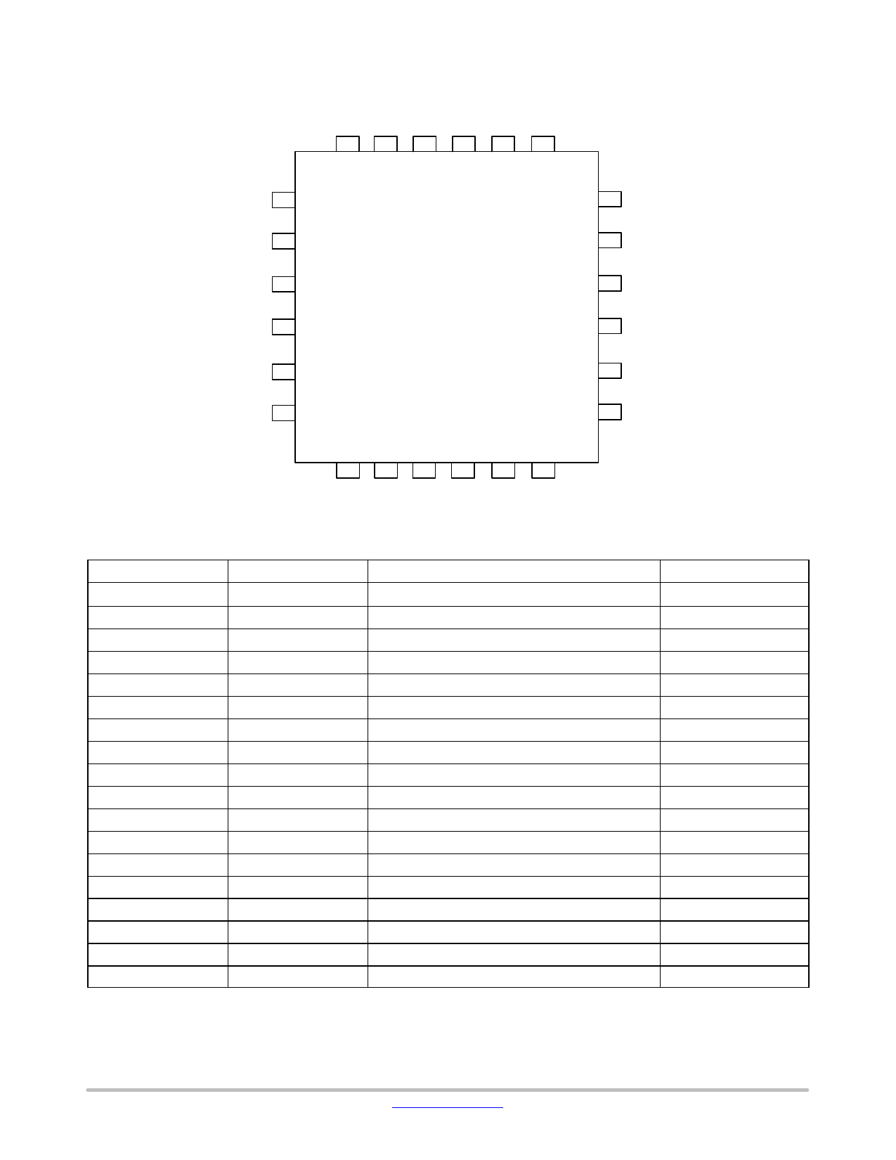
PACKAGE AND PIN DESCRIPTION
24 23 22 21 20 19
1 TEST
2 TEST1
3 VBOOSTM3V
4 VBOOST
5 TEST2
6 GND
NCV78713
VDD 18
SDI 17
SCLK 16
CSB 15
SDO 14
RSTB 13
7 8 9 10 11 12
Figure 4. Pin Connections
Table 2. PIN DESCRIPTION
Pin No.
Pin Name
1 TEST
2 TEST1
3 VBOOSTM3V
4 VBOOST
5 TEST2
6 GND
7 VLED
8 LBCKSW
9, 11
GND/NC
10 VINBCK
12 LEDCTRL
13 RSTB
14 SDO
15 CSB
16 SCLK
17 SDI
18 VDD
19, 20, 21, 22, 23, 24
NC
Description
Test Pin
Test Pin
VBOOSTM3V Regulator Output Pin
Booster Input Voltage Pin
Test Pin
Ground
LED String Forward Voltage Sense Input
Buck Switch Output
GND/NC Connection in Application
Buck High Voltage Supply
LED String Enable
External Reset Signal
SPI Data Output
SPI Chip Select (Chip Select Bar)
SPI Clock
SPI Data Input
3 V Logic Supply
GND/NC Connection in the Application
I/O Type
LV In
LV IN/OUT HV Tolerant
HV OUT (Supply)
HV Supply
LV IN/OUT HV Tolerant
Ground
HV IN
HV OUT
NC
HV Supply
MV IN
MV IN
MV Open-Drain
MV IN
MV IN
MV IN
LV Supply
NC
www.onsemi.com
5
5 Page 
NCV78713
Table 6. ELECTRICAL CHARACTERISTICS (continued)
(All Min and Max parameters are guaranteed over full junction temperature (TJP) range (−40°C; 150°C), unless otherwise specified)
Characteristic
Symbol
Condition
Min Typ
Max Unit
3 V DIGITAL INPUTS (TEST, TEST1, TEST2)
High-Level Input Voltage
VIN3HI
2.3 −
−V
Low-Level Input Voltage
VIN3LO
− − 0.8 V
Pull Resistance
SPI INTERFACE
RPD3
Pull-Down Resistance
− − 60 kW
CSB Setup Time
CSB Hold Time
SCLK Low Time
SCLK High Time
Data-In (DIN) Setup Time,
Valid Data before Rising Edge
of CLK
tCSS
tCSH
tWL
tWH
tSU
0.5 −
0.25 −
0.5 −
0.5 −
0.25 −
− ms
− ms
− ms
− ms
− ms
Data-In (DIN) Hold Time, Hold
Data after Rising Edge of CLK
tH
0.275
−
− ms
Output (DOUT) Disable Time
(Note 23)
tDIS
0.08 −
0.32 ms
Output (DOUT) Valid
(Note 23)
tV1→0
− − 0.32 ms
Output (DOUT) Valid
(Note 24)
tV0→1
−
−
0.32 +
ms
t(RC)
Output (DOUT) Hold Time
tHO
0.01 −
− ms
CSB High Time
tCS
1 − − ms
Product parametric performance is indicated in the Electrical Characteristics for the listed test conditions, unless otherwise noted. Product
performance may not be indicated by the Electrical Characteristics if operated under different conditions.
23. SDO low-side switch activation time.
24. Time depends on the SDO load and pull-up resistor.
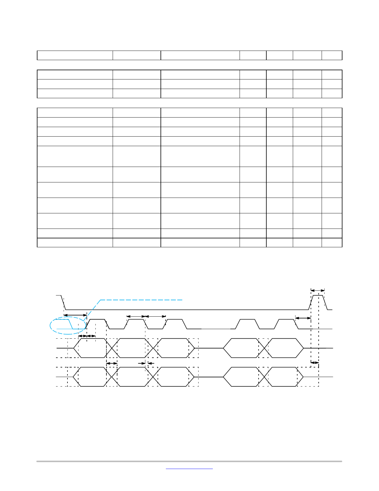
Initial State of SCLK after CSB Falling Edge
VIH is Don’t Care, It Can be Low or High
CSB
VIL tCSS
VIH
tWH tWL
SCLK
VIL
VIH
ÉÉ ÉÉ ÉÉ ÉÉDIN
ÉÉ ÉÉ ÉÉ ÉÉVIL
ÉÉ ÉÉ ÉÉ ÉÉVIH
ÉÉ ÉÉ ÉÉ ÉÉDOUT
ÉÉ ÉÉ ÉÉ ÉÉHI−Z
ÉÉ ÉÉ ÉÉ ÉÉVIL
tSU tH
DIN15
DOUT15
DIN14
tV
DOUT14
DIN13
tHO
DOUT13
tCS
tCSH
ÉÉDIN1
DIN0
ÉÉÉÉÉÉÉÉÉÉ ÉÉÉÉÉÉÉÉÉDOUT1
DOUT0
tDIS
HI−Z
Figure 5. SPI Communication Timing
www.onsemi.com
11
11 Page | ||
| Páginas | Total 30 Páginas | |
| PDF Descargar | [ Datasheet NCV78713.PDF ] | |
Hoja de datos destacado
| Número de pieza | Descripción | Fabricantes |
| NCV78713 | High Efficiency Buck Single LED Driver | ON Semiconductor |
| Número de pieza | Descripción | Fabricantes |
| SLA6805M | High Voltage 3 phase Motor Driver IC. |
Sanken |
| SDC1742 | 12- and 14-Bit Hybrid Synchro / Resolver-to-Digital Converters. |
Analog Devices |
|
DataSheet.es es una pagina web que funciona como un repositorio de manuales o hoja de datos de muchos de los productos más populares, |
| DataSheet.es | 2020 | Privacy Policy | Contacto | Buscar |
