|
|
|
PDF FDQ7238AS Data sheet ( Hoja de datos )
| Número de pieza | FDQ7238AS | |
| Descripción | Dual Notebook Power Supply N-Channel PowerTrench | |
| Fabricantes | Fairchild Semiconductor | |
| Logotipo | ||
Hay una vista previa y un enlace de descarga de FDQ7238AS (archivo pdf) en la parte inferior de esta página. Total 9 Páginas | ||
|
No Preview Available !
May 2008
FDQ7238AS
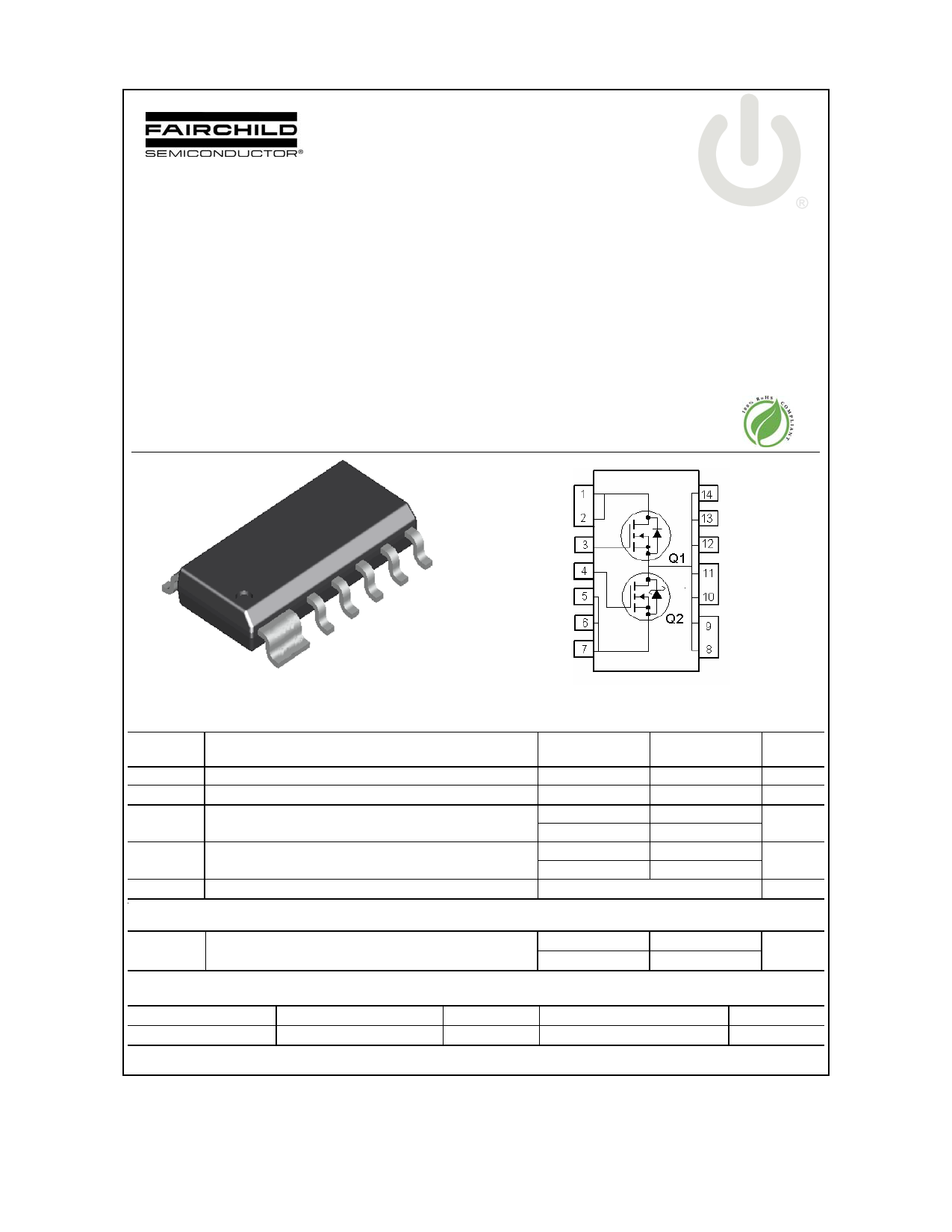
Dual Notebook Power Supply N-Channel PowerTrench® in SO-14 Package
General Description
The FDQ7238AS is designed to replace two single SO-
8 MOSFETs in DC to DC power supplies. The high-side
switch (Q1) is designed with specific emphasis on
reducing switching losses while the low-side switch
(Q2) is optimized to reduce conduction losses using
Fairchild’s SyncFET TM technology. The FDQ7238AS
includes a patented combination of a MOSFET
monolithically integrated with a Schottky diode.
Features
• Q2: 14 A, 30V. RDS(on) = 8.7 mΩ @ VGS = 10V
RDS(on) = 10.5 mΩ @ VGS = 4.5V
• Q1: 11 A, 30V. RDS(on) = 13.2 mΩ @ VGS = 10V
RDS(on) = 16 mΩ @ VGS = 4.5V
SO-14
pin 1
S2
S2
S2
G1G2
Vin
Absolute Maximum Ratings TA = 25°C unless otherwise noted
Symbol
VDSS
VGSS
ID
PD
TJ, TSTG
Parameter
Drain-Source Voltage
Gate-Source Voltage
Drain Current - Continuous
- Pulsed
Power Dissipation for Single Operation
(Note 1a)
(Note 1a & 1b)
(Note 1c & 1d)
Operating and Storage Junction Temperature Range
Thermal Characteristics
RθJA Thermal Resistance, Junction-to-Ambient (Note 1a & 1b)
(Note 1c & 1d)
Package Marking and Ordering Information
Device Marking
FDQ7238AS
Device
FDQ7238AS
Reel Size
13”
Q2 Q1
30 30
±20 ±20
14 11
50 50
2.4 1.8
1.3 1.1
−55 to +150
52 68
94 118
Units
V
V
A
W
°C
°C/W
Tape width
16mm
Quantity
2500 units
©2008 Fairchild Semiconductor Corporation
FDQ7238AS Rev A1(X)
1 page 
Typical Characteristics : Q2
10
ID = 14A
8
6
4
VDS = 10V
20V
15V
2
0
0 5 10 15 20 25 30
Qg, GATE CHARGE (nC)
Figure 7. Gate Charge Characteristics.
100
RDS(ON) LIMIT
10
1
100µs
1ms
10ms
100ms
1s
10s
DC
VGS = 10V
0.1 SINGLE PULSE
RθJA = 94oC/W
TA = 25oC
0.01
0.01
0.1 1 10
VDS, DRAIN-SOURCE VOLTAGE (V)
100
Figure 9. Maximum Safe Operating Area.
2500
2000
1500
f = 1MHz
VGS = 0 V
Ciss
1000
500
Crss
0
0
Coss
5 10 15 20 25
VDS, DRAIN TO SOURCE VOLTAGE (V)
30
Figure 8. Capacitance Characteristics.
50
SINGLE PULSE
RθJA = 94°C/W
40 TA = 25°C
30
20
10
0
0.001
0.01
0.1 1 10
t1, TIME (sec)
100
Figure 10. Single Pulse Maximum
Power Dissipation.
1000
1
0.1
0.01
D = 0.5
0.2
0.1
0.05
0.02
0.01
SINGLE PULSE
0.001
0.0001
0.001
0.01
0.1 1
t1, TIME (sec)
RθJA(t) = r(t) * RθJA
RθJA = 94°C/W
P(pk)
t1
t2
TJ - TA = P * RθJA(t)
Duty Cycle, D = t1 / t2
10 100 1000
Figure 11. Transient Thermal Response Curve.
Thermal characterization performed using the conditions described in Note 1d.
Transient thermal response will change depending on the circuit board design
FDQ7238AS Rev A1 (X)
5 Page | ||
| Páginas | Total 9 Páginas | |
| PDF Descargar | [ Datasheet FDQ7238AS.PDF ] | |
Hoja de datos destacado
| Número de pieza | Descripción | Fabricantes |
| FDQ7238AS | Dual Notebook Power Supply N-Channel PowerTrench | Fairchild Semiconductor |
| Número de pieza | Descripción | Fabricantes |
| SLA6805M | High Voltage 3 phase Motor Driver IC. |
Sanken |
| SDC1742 | 12- and 14-Bit Hybrid Synchro / Resolver-to-Digital Converters. |
Analog Devices |
|
DataSheet.es es una pagina web que funciona como un repositorio de manuales o hoja de datos de muchos de los productos más populares, |
| DataSheet.es | 2020 | Privacy Policy | Contacto | Buscar |