|
|
|
PDF NTMFS4933N Data sheet ( Hoja de datos )
| Número de pieza | NTMFS4933N | |
| Descripción | Power MOSFET ( Transistor ) | |
| Fabricantes | ON Semiconductor | |
| Logotipo | ||
Hay una vista previa y un enlace de descarga de NTMFS4933N (archivo pdf) en la parte inferior de esta página. Total 7 Páginas | ||
|
No Preview Available !
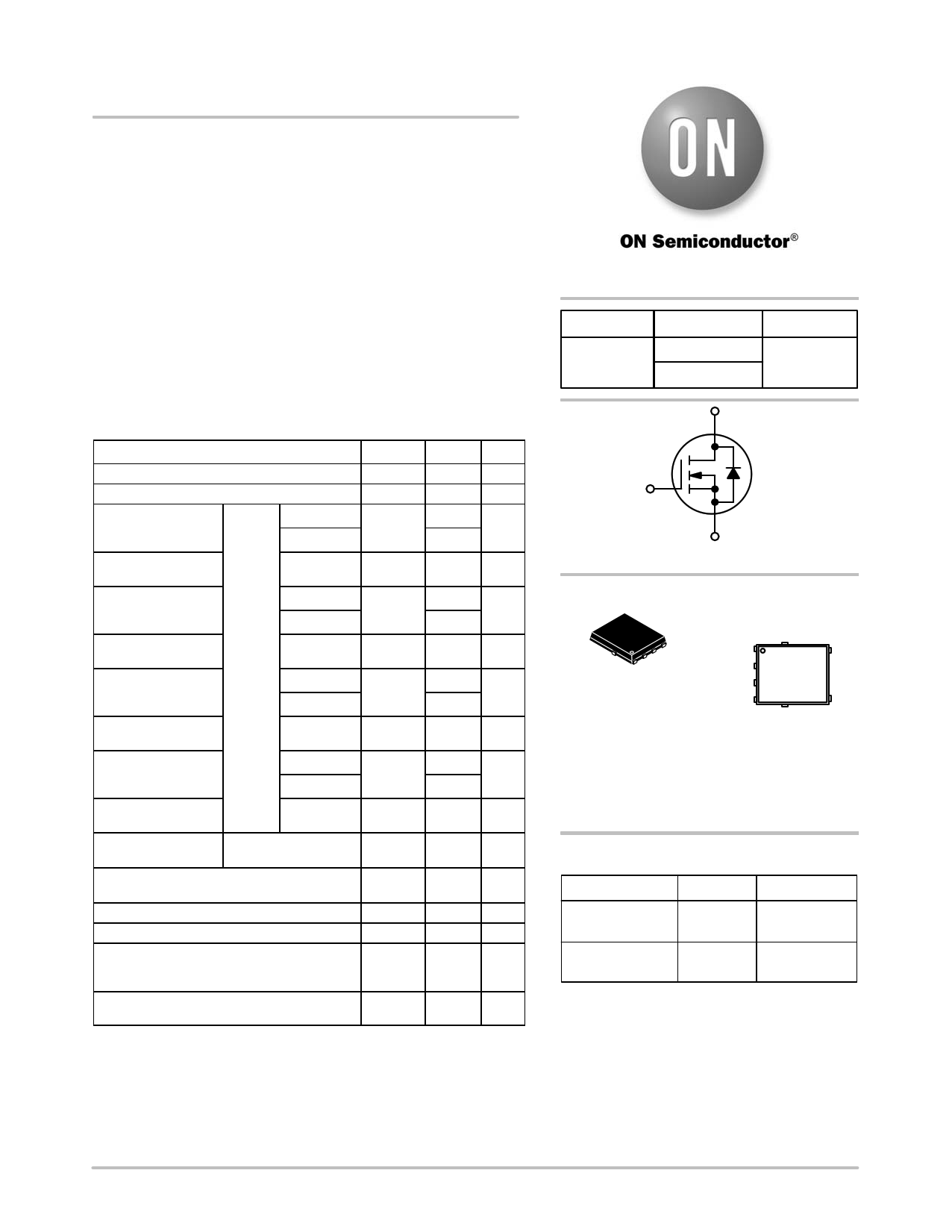
NTMFS4933N
Power MOSFET
30 V, 210 A, Single N−Channel, SO−8 FL
Features
• Low RDS(on) to Improve Conduction and Overall Efficiency
• These Devices are Pb−Free, Halogen Free/BFR Free and are RoHS
Compliant
Applications
• OR−ing FET, Power Load Switch, Motor Control
• Refer to Application Note AND8195/D for Mounting Information
End Products
• Server, UPS, Fault−Tolerant Power Systems, Hot Swap
MAXIMUM RATINGS (TJ = 25°C unless otherwise stated)
Parameter
Symbol Value Unit
Drain−to−Source Voltage
Gate−to−Source Voltage
Continuous Drain
C(Nuortreen1t)RqJA
TA = 25°C
TA = 100°C
VDSS
VGS
ID
30
±20
34
21.5
V
V
A
Power Dissipation
RqJA (Note 1)
Continuous Drain
C(Nuortreen1t)RqJA ≤ 10 s
TA = 25°C
TA = 25°C
TA = 100°C
PD
ID
2.74 W
43 A
27
Power Dissipation
RqJA ≤ 10 s (Note 1)
Continuous Drain
C(Nuortreen2t)RqJA
Steady
State
TA = 25°C
TA = 25°C
TA = 100°C
PD
ID
7.3 W
20 A
12.5
Power Dissipation
RqJA (Note 2)
Continuous Drain
C(Nuortreen1t)RqJC
TA = 25°C
TC = 25°C
TC =100°C
PD
ID
1.06 W
210 A
132
Power Dissipation
RqJC (Note 1)
Pulsed Drain
Current
TC = 25°C
TA = 25°C, tp = 10 ms
PD
IDM
104 W
400 A
Operating Junction and Storage
Temperature
Source Current (Body Diode)
Drain to Source DV/DT
Single Pulse Drain−to−Source Avalanche
Energy (TJ = 25°C, VDD = 24 V, VGS = 10 V,
IL = 58 Apk, L = 0.3 mH, RG = 25 W)
Lead Temperature for Soldering Purposes
(1/8″ from case for 10 s)
TJ,
TSTG
IS
dV/dt
EAS
−55 to
+150
95
4.4
504
°C
A
V/ns
mJ
TL 260 °C
Stresses exceeding Maximum Ratings may damage the device. Maximum
Ratings are stress ratings only. Functional operation above the Recommended
Operating Conditions is not implied. Extended exposure to stresses above the
Recommended Operating Conditions may affect device reliability.
1. Surface−mounted on FR4 board using 1 sq−in pad, 1 oz Cu.
2. Surface−mounted on FR4 board using the minimum recommended pad size.
(Cu area = 50 mm2 [1 oz])
http://onsemi.com
V(BR)DSS
30 V
RDS(ON) MAX
1.2 mW @ 10 V
2.0 mW @ 4.5 V
D (5,6)
ID MAX
210 A
G (4)
S (1,2,3)
N−CHANNEL MOSFET
MARKING
DIAGRAM
1
SO−8 FLAT LEAD
CASE 488AA
STYLE 1
D
S
S
S
4933N
AYWZZ
D
GD
D
A = Assembly Location
Y = Year
W = Work Week
ZZ = Lot Traceability
ORDERING INFORMATION
Device
NTMFS4933NT1G
Package
SO−8 FL
(Pb−Free)
Shipping†
1500 /
Tape & Reel
NTMFS4933NT3G SO−8 FL
(Pb−Free)
5000 /
Tape & Reel
†For information on tape and reel specifications,
including part orientation and tape sizes, please
refer to our Tape and Reel Packaging Specifications
Brochure, BRD8011/D.
© Semiconductor Components Industries, LLC, 2012
May, 2012 − Rev. 8
1
Publication Order Number:
NTMFS4933N/D
1 page 
13000
12000
11000
10000
9000
8000
7000
6000
5000
4000
3000
2000
1000
0
0
NTMFS4933N
TYPICAL CHARACTERISTICS
Ciss
TJ = 25°C
VGS = 0 V
Coss
Crss
5 10 15 20 25
VDS, DRAIN−TO−SOURCE VOLTAGE (V)
Figure 7. Capacitance Variation
30
10
9
8 TJ = 25°C
7 QT
6
5
4
3 QGS
2 QGD
1
0
VDD = 15 V
VGS = 10 V
ID = 30 A
0 20 40 60 80 100 120 140
QG, TOTAL GATE CHARGE (nC)
Figure 8. Gate−To−Source and Drain−To−Source
Voltage vs. Total Charge
10000
1000
VDD = 15 V
ID = 15 A
VGS = 10 V
100
10
td(off)
tf
tr
td(on)
1
1 10 100
RG, GATE RESISTANCE (W)
Figure 9. Resistive Switching Time
Variation vs. Gate Resistance
30
VGS = 0 V
25
20
TJ = 125°C
15
10
TJ = 25°C
5
0
0.4 0.5 0.6 0.7 0.8 0.9 1.0
VSD, SOURCE−TO−DRAIN VOLTAGE (V)
Figure 10. Diode Forward Voltage vs. Current
1000
100 10 ms
100 ms
10 1 ms
0 V ≤ VGS ≤ 20 V
1 SINGLE PULSE
TA = 25°C
TJ = 150°C
0.1 RDS(on) LIMIT
THERMAL LIMIT
10 ms
100 ms
dc
0.01
0.01
PACKAGE LIMIT
0.1 1
10 100
VDS, DRAIN−TO−SOURCE VOLTAGE (V)
Figure 11. Maximum Rated Forward Biased
Safe Operating Area
520
480 ID = 58 A
440
400
360
320
280
240
200
160
120
80
40
0
25 50 75 100 125 150
TJ, STARTING JUNCTION TEMPERATURE (°C)
Figure 12. Maximum Avalanche Energy vs.
Starting Junction Temperature
http://onsemi.com
5
5 Page | ||
| Páginas | Total 7 Páginas | |
| PDF Descargar | [ Datasheet NTMFS4933N.PDF ] | |
Hoja de datos destacado
| Número de pieza | Descripción | Fabricantes |
| NTMFS4933N | Power MOSFET ( Transistor ) | ON Semiconductor |
| Número de pieza | Descripción | Fabricantes |
| SLA6805M | High Voltage 3 phase Motor Driver IC. |
Sanken |
| SDC1742 | 12- and 14-Bit Hybrid Synchro / Resolver-to-Digital Converters. |
Analog Devices |
|
DataSheet.es es una pagina web que funciona como un repositorio de manuales o hoja de datos de muchos de los productos más populares, |
| DataSheet.es | 2020 | Privacy Policy | Contacto | Buscar |