|
|
|
PDF LTM8047 Data sheet ( Hoja de datos )
| Número de pieza | LTM8047 | |
| Descripción | uModule DC/DC Converter | |
| Fabricantes | Linear Technology | |
| Logotipo | ||
Hay una vista previa y un enlace de descarga de LTM8047 (archivo pdf) en la parte inferior de esta página. Total 18 Páginas | ||
|
No Preview Available !
LTM8047
3.1VIN to 32VIN Isolated
µModule DC/DC Converter
FEATURES
n Complete Switch Mode Power Supply
n 725VDC Isolation
n Wide Input Voltage Range: 3.1V to 32V
n Up to 440mA Output Current (VOUT = 2.5V)
n 2.5V to 12V Output Voltage
n Current Mode Control
n Programmable Soft-Start
n User Configurable Undervoltage Lockout
n SnPb or RoHS Compliant Finish
n Low Profile (11.25mm × 9mm × 4.92mm) Surface
Mount BGA Package
APPLICATIONS
n Industrial Sensors
n Industrial Switches
n Ground Loop Mitigation
DESCRIPTION
The LTM®8047 is an isolated flyback µModule DC/DC
converter. The LTM8047 has an isolation rating of 725VDC.
For a similar product with LDO post regulator, see the
LTM8048. Included in the package are the switching
controller, power switches, transformer, and all support
components. Operating over an input voltage range of 3.1V
to 32V, the LTM8047 supports an output voltage range of
2.5V to 12V, set by a single resistor. Only output, input,
and bypass capacitors are needed to finish the design.
Other components may be used to control the soft-start
control and biasing.
The LTM8047 is packaged in a thermally enhanced, com-
pact (11.25mm × 9mm × 4.92mm) over-molded ball grid
array (BGA) package suitable for automated assembly by
standard surface mount equipment. The LTM8047 is avail-
able with SnPb (BGA) or RoHS compliant terminal finish.
L, LT, LTC, LTM, Linear Technology, the Linear logo and µModule are registered trademarks of
Linear Technology Corporation. All other trademarks are the property of their respective owners.
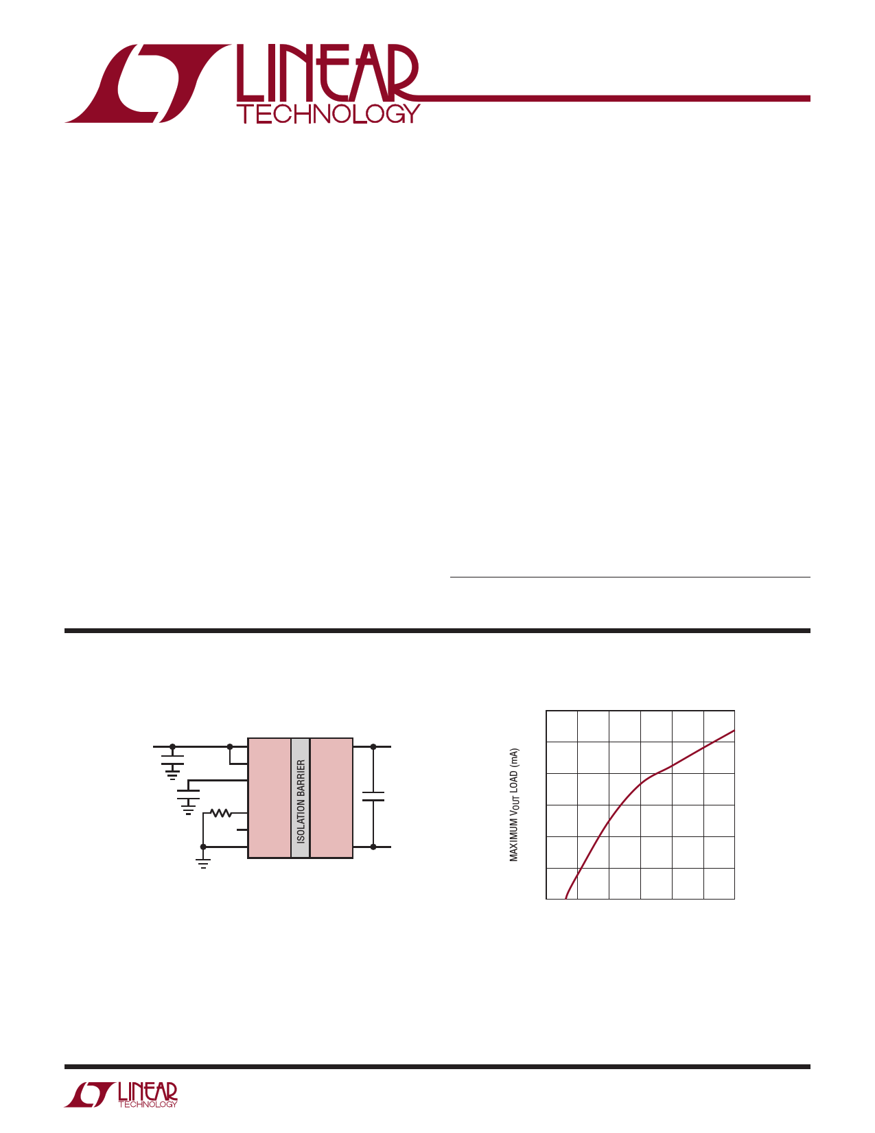
TYPICAL APPLICATION
725V DC Isolated Low Noise µModule Regulator
VIN
3.1V TO 29V
2.2µF
4.7µF
6.98k
VIN
RUN
BIAS
LTM8047
VOUT
ADJ
SS
GND VOUT–
725VDC ISOLATION
VOUT
5V
280mA
(15VIN)
22µF
8047 TA01
400
350
300
250
200
150
100
0
Maximum Load vs VIN
5 10 15 20 25 30
VIN (V)
8047 TA01b
For more information www.linear.com/LTM8047
8047fc
1
1 page 
TYPICAL PERFORMANCE CHARACTERISTICS
LTM8047
Minimum Load vs VIN
40 2.5VOUT
35
3.3VOUT
5VOUT
30
25
20
15
10
5
0
0 5 10 15 20
VIN (V)
25 30
8047 G13
Junction Temperature Rise vs
Load Current
8 VOUT = 2.5V
7
6
5
4
3
2 3.3VIN
1
5VIN
12VIN
0 24VIN
0 50 100 150 200 250 300 350 400
VOUT LOAD CURRENT (mA)
8047 G16
Junction Temperature Rise vs
Load Current
12 VOUT = 8V
10
8
6
4
3.3VIN
2 5VIN
12VIN
0 24VIN
0 50 100 150 200 250 300
VOUT LOAD CURRENT (mA)
8047 G19
Minimum Load vs VIN
15 8VOUT1
12VOUT1
12
9
6
3
0
0 5 10 15 20 25 30
VIN (V)
8047 G14
Input
VOUT
Current
Shorted
vs
VIN
80
70
60
50
40
30
20
10
0 4 8 12 16 20 24 28 32
VIN (V)
8047 G15
Junction Temperature Rise vs
Load Current
9 VOUT = 3.3V
8
7
6
5
4
3
2
3.3VIN
5VIN
1 12VIN
0 24VIN
0 50 100 150 200 250 300 350 400
VOUT LOAD CURRENT (mA)
8047 G17
Junction Temperature Rise vs
Load Current
10
9
VOUT = 5V
8
7
6
5
4
3
2
3.3VIN
5VIN
1
0
12VIN
24VIN
0 50 100 150 200 250 300 350
VOUT LOAD CURRENT (mA)
8047 G18
Junction Temperature Rise vs
Load Current
12 VOUT = 12V
10
8
Output Noise and Ripple
10mV/DIV
6
4
3.3VIN
2 5VIN
12VIN
0 24VIN
0 50 100 150 200 250
VOUT LOAD CURRENT (mA)
8047 G20
2µs/DIV
8047 G21
12VIN, 5VOUT at 250mA
0B.E1TμWF E2E5N0VGSNADFAETNYDCVAOPUATC–ITOR APPLIED
For more information www.linear.com/LTM8047
8047fc
5
5 Page 
LTM8047
APPLICATIONS INFORMATION
LTM8047 Line Regulation
12VOUT, 15mA Output Current
12.50
12.25
NO CAP
12pF
18pF
12.00
11.75
VOUT
COUT
LTM8047
ADJ
SS
BIAS
11.50
11.25
11.00
VOUT–
GND
RUN
10.75
0
5 10 15 20 25
VIN (V)
8047 F01
Figure 1. For higher output voltages, the LTM8047 requires some
capacitance from ADJ to GND for proper line regulation
VOUT to VOUT– Reverse Voltage
TtohVeOLUTTM–8d0u4ri7ncgaonpneortattoiolenr.aItfeVaOUreTv–errasiseevsoaltbaogveefrVoOmUTVdOuUrT-
ing operation, the LTM8047 may be damaged. To protect
against this condition, a low forward drop power Schottky
diode has been integrated into the LTM8047, anti-parallel
to VOUT/VOUT–. This can protect the output against many
reverse voltage faults. Reverse voltage faults can be both
steady state and transient. An example of a steady state
voltage reversal is accidentally misconnecting a powered
LTM8047 to a negative voltage source. An example of
transient voltage reversals is a momentary connection to
a negative voltage. It is also possible to achieve a VOUT
reversal if the load is short-circuited through a long cable.
The inductance of the long cable forms an LC tank circuit
with the VOUT capacitance, which drives VOUT negative.
Avoid these conditions.
PCB Layout
CIN VIN
THERMAL/INTERCONNECT VIAS
8047 F02
Figure 2. Layout Showing Suggested External Components,
Planes and Thermal Vias
A few rules to keep in mind are:
1. Place the RADJ resistor as close as possible to its re-
spective pin.
2. Place the CIN capacitor as close as possible to the VIN
and GND connections of the LTM8047.
3. aPnladceVOthUeT–C. OUT capacitor as close as possible to VOUT
4. Place the CIN and COUT capacitors such that their
ground current flow directly adjacent or underneath
the LTM8047.
5. Connect all of the GND connections to as large a copper
pour or plane area as possible on the top layer. Avoid
breaking the ground connection between the external
components and the LTM8047.
Most of the headaches associated with PCB layout have 6. Use vias to connect the GND copper area to the board’s
been alleviated or even eliminated by the high level of
internal ground planes. Liberally distribute these GND
integration of the LTM8047. The LTM8047 is neverthe-
less a switching power supply, and care must be taken to
vias to provide both a good ground connection and
thermal path to the internal planes of the printed circuit
minimize electrical noise to ensure proper operation. Even
board. Pay attention to the location and density of the
with the high level of integration, you may fail to achieve
specified operation with a haphazard or poor layout. See
thermal vias in Figure 2. The LTM8047 can benefit from
the heat sinking afforded by vias that connect to internal
Figure 2 for a suggested layout. Ensure that the grounding
GND planes at these locations, due to their proximity
and heat sinking are acceptable.
to internal power handling components. The optimum
8047fc
For more information www.linear.com/LTM8047
11
11 Page | ||
| Páginas | Total 18 Páginas | |
| PDF Descargar | [ Datasheet LTM8047.PDF ] | |
Hoja de datos destacado
| Número de pieza | Descripción | Fabricantes |
| LTM8040 | 1A Module LED Driver | Linear Technology |
| LTM8042 | uModule Boost LED Driver and Current Source | Linear Technology |
| LTM8042-1 | uModule Boost LED Driver and Current Source | Linear Technology |
| LTM8045 | Inverting or SEPIC uModule DC/DC Converter | Linear Technology |
| Número de pieza | Descripción | Fabricantes |
| SLA6805M | High Voltage 3 phase Motor Driver IC. |
Sanken |
| SDC1742 | 12- and 14-Bit Hybrid Synchro / Resolver-to-Digital Converters. |
Analog Devices |
|
DataSheet.es es una pagina web que funciona como un repositorio de manuales o hoja de datos de muchos de los productos más populares, |
| DataSheet.es | 2020 | Privacy Policy | Contacto | Buscar |