|
|
|
PDF ADuM231E Data sheet ( Hoja de datos )
| Número de pieza | ADuM231E | |
| Descripción | 5.0 kV RMS Triple Channel Digital Isolators | |
| Fabricantes | Analog Devices | |
| Logotipo | ||
Hay una vista previa y un enlace de descarga de ADuM231E (archivo pdf) en la parte inferior de esta página. Total 19 Páginas | ||
|
No Preview Available !
Data Sheet
5.0 kV RMS Triple Channel Digital Isolators
ADuM230D/ADuM230E/ADuM231D/ADuM231E
FEATURES
High common-mode transient immunity: 100 kV/µs
High robustness to radiated and conducted noise
Low propagation delay: 13 ns maximum for 5 V operation,
15 ns maximum for 1.8 V operation
150 Mbps maximum data rate
Safety and regulatory approvals (pending)
UL recognition
5000 V rms for 1 minute per UL 1577
CSA Component Acceptance Notice 5A
VDE certificate of conformity
DIN V VDE V 0884-10 (VDE V 0884-10):2006-12
VIORM = 849 V peak
8000 V peak reinforced surge isolation voltage (VIOSM)
CQC certification per GB4943.1-2011
Low dynamic power consumption
1.8 V to 5 V level translation
High temperature operation: 125°C
Fail-safe high or low options
16-lead, RoHS-compliant, SOIC package
APPLICATIONS
General-purpose multichannel isolation
Serial peripheral interface (SPI)/data converter isolation
Industrial field bus isolation
GENERAL DESCRIPTION
The ADuM230D/ADuM230E/ADuM231D/ADuM231E1 are
triple-channel digital isolators based on Analog Devices, Inc.,
iCoupler® technology. Combining high speed, complementary
metal-oxide semiconductor (CMOS) and monolithic air core
transformer technology, these isolation components provide
outstanding performance characteristics superior to alternatives
such as optocoupler devices and other integrated couplers. The
maximum propagation delay is 13 ns with a pulse width
distortion of less than 3 ns at 5 V operation. Channel matching
is tight at 3.0 ns maximum.
The ADuM230D/ADuM230E/ADuM231D/ADuM231E data
channels are independent and are available in a variety of
configurations with a withstand voltage rating of 5.0 kV rms
(see the Ordering Guide). The devices operate with the supply
voltage on either side ranging from 1.8 V to 5 V, providing
compatibility with lower voltage systems as well as enabling
voltage translation functionality across the isolation barrier.
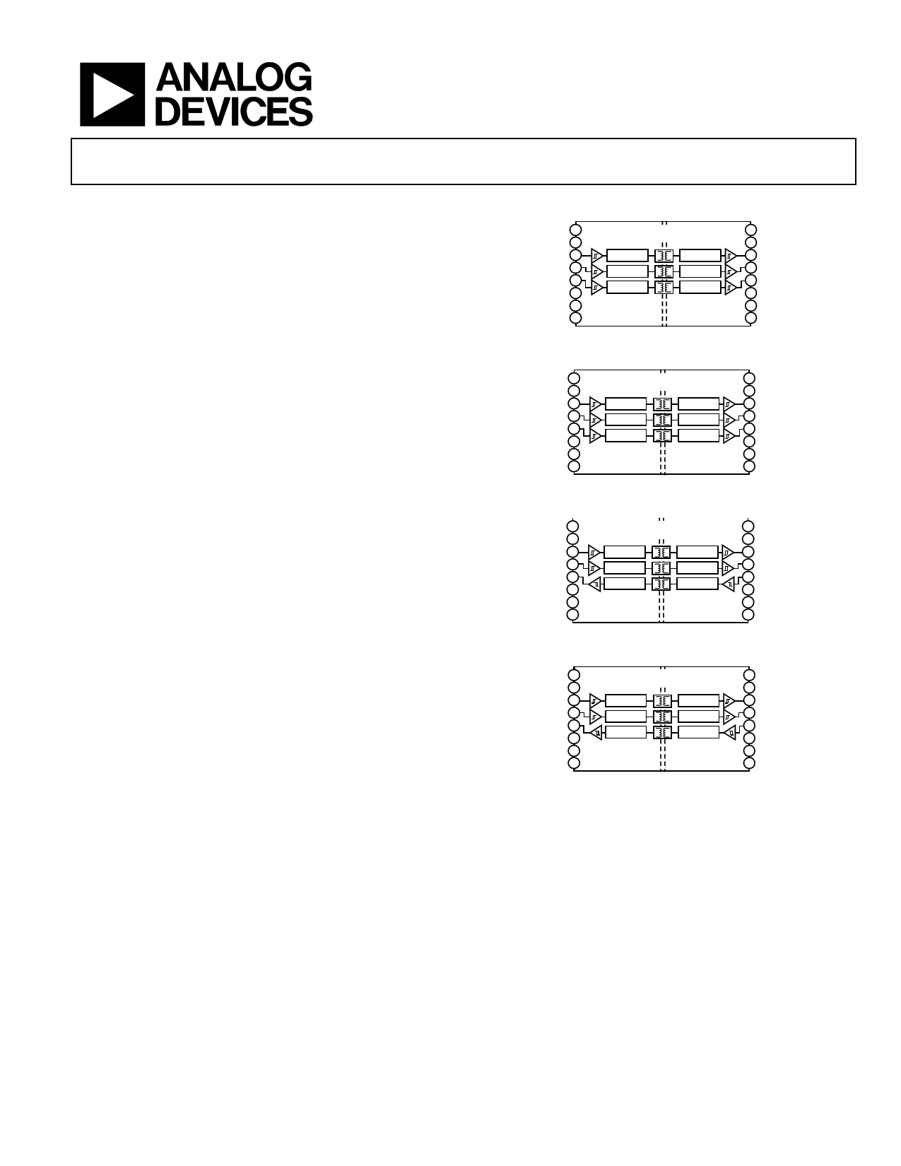
FUNCTIONAL BLOCK DIAGRAMS
VDD1 1
GND1 2
VIA 3
VIB 4
VIC 5
NIC 6
DISABLE1 7
GND1 8
ADuM230D
ENCODE
ENCODE
ENCODE
DECODE
DECODE
DECODE
16 VDD2
15 GND2
14 VOA
13 VOB
12 VOC
11 NIC
10 NIC
9 GND2
NIC = NO INTERNAL CONNECTION. LEAVE THIS PIN FLOATING.
Figure 1. ADuM230D Functional Block Diagram
VDD1 1
GND1 2
VIA 3
VIB 4
VIC 5
NIC 6
ADuM230E
ENCODE
ENCODE
ENCODE
DECODE
DECODE
DECODE
16 VDD2
15 GND2
14 VOA
13 VOB
12 VOC
11 NIC
NIC 7
GND1 8
10 VE2
9 GND2
NIC = NO INTERNAL CONNECTION. LEAVE THIS PIN FLOATING.
Figure 2. ADuM230E Functional Block Diagram
VDD1 1
GND1 2
VIA 3
VIB 4
VOC 5
NIC 6
DISABLE1 7
GND1 8
ADuM231D
ENCODE
ENCODE
DECODE
DECODE
DECODE
ENCODE
16 VDD2
15 GND2
14 VOA
13 VOB
12 VIC
11 NIC
10 DISABLE2
9 GND2
NIC = NO INTERNAL CONNECTION. LEAVE THIS PIN FLOATING.
Figure 3. ADuM231D Functional Block Diagram
VDD1 1
GND1 2
VIA 3
VIB 4
VOC 5
NIC 6
VE1 7
GND1 8
ADuM231E
ENCODE
ENCODE
DECODE
DECODE
DECODE
ENCODE
16 VDD2
15 GND2
14 VOA
13 VOB
12 VIC
11 NIC
10 VE2
9 GND2
NIC = NO INTERNAL CONNECTION. LEAVE THIS PIN FLOATING.
Figure 4. ADuM231E Functional Block Diagram
Unlike other optocoupler alternatives, dc correctness is ensured
in the absence of input logic transitions. Two different fail-safe
options are available, by which the outputs transition to a
predetermined state when the input power supply is not applied
or the inputs are disabled.
1 Protected by U.S. Patents 5,952,849; 6,873,065; 6,903,578; and 7,075,329. Other patents are pending.
Rev. 0
Document Feedback
Information furnished by Analog Devices is believed to be accurate and reliable. However, no
responsibilityisassumedbyAnalogDevices for itsuse,nor foranyinfringementsofpatentsor other
rights of third parties that may result from its use. Specifications subject to change without notice. No
license is granted by implication or otherwise under any patent or patent rights of Analog Devices.
Trademarksandregisteredtrademarksarethepropertyoftheirrespectiveowners.
One Technology Way, P.O. Box 9106, Norwood, MA 02062-9106, U.S.A.
Tel: 781.329.4700
©2015 Analog Devices, Inc. All rights reserved.
Technical Support
www.analog.com
1 page 
Data Sheet
ADuM230D/ADuM230E/ADuM231D/ADuM231E
Parameter
Output Voltage
Logic High
Logic Low
Input Current per Channel
VE2 Enable Input Pull-Up Current
DISABLE1 Input Pull-Down Current
Tristate Output Current per Channel
Quiescent Supply Current
ADuM230D/ADuM230E
ADuM231D/ADuM231E
Dynamic Supply Current
Dynamic Input
Dynamic Output
Undervoltage Lockout
Positive VDDx Threshold
Negative VDDx Threshold
VDDx Hysteresis
AC SPECIFICATIONS
Output Rise/Fall Time
Common-Mode Transient Immunity7
Symbol
VOH
VOL
II
IPU
IPD
IOZ
IDD1 (Q)
IDD2 (Q)
IDD1 (Q)
IDD2 (Q)
IDD1 (Q)
IDD2 (Q)
IDD1 (Q)
IDD2 (Q)
IDDI (D)
IDDO (D)
UVLO
VDDxUV+
VDDxUV−
VDDxUVH
tR/tF
|CMH|
Min
VDDx − 0.1
VDDx − 0.4
−10
−10
−10
75
Typ
VDDx
VDDx − 0.2
0.0
0.2
+0.01
−3
9
+0.01
1.25
1.65
9.57
1.79
1.52
1.52
7.28
5.24
0.01
0.01
1.6
1.5
0.1
2.5
100
Max
0.1
0.4
+10
15
+10
2.5
2.8
15.0
2.9
2.6
2.6
11.3
7.1
|CML|
75
100
Unit
V
V
V
V
µA
µA
µA
µA
Test Conditions/Comments
IOx2 = −20 µA, VIx = VIxH3
IOx2 = −2 mA, VIx = VIxH3
IOx2 = 20 µA, VIx = VIxL4
IOx2 = 2 mA, VIx = VIxL4
0 V ≤ VIx ≤ VDDx
VE2 = 0 V
DISABLE1 = VDDx
0 V ≤ VOx ≤ VDDx
mA VI5 = 0 (E0, D0), 1 (E1, D1)6
mA VI5 = 0 (E0, D0), 1 (E1, D1)6
mA VI5 = 1 (E0, D0), 0 (E1, D1)6
mA VI5 = 1 (E0, D0), 0 (E1, D1)6
mA VI5 = 0 (E0, D0), 1 (E1, D1)6
mA VI5 = 0 (E0, D0), 1 (E1, D1)6
mA VI5 = 1 (E0, D0), 0 (E1, D1)6
mA VI5 = 1 (E0, D0), 0 (E1, D1)6
mA/Mbps Inputs switching, 50% duty cycle
mA/Mbps Inputs switching, 50% duty cycle
V
V
V
ns
kV/µs
kV/µs
10% to 90%
VIx = VDDx, VCM = 1000 V,
transient magnitude = 800 V
VIx = 0 V, VCM = 1000 V,
transient magnitude = 800 V
1 150 Mbps is the highest data rate that can be guaranteed, although higher data rates are possible.
2 IOx is the Channel x output current, where x = A, B, or C.
3 VIxH is the input side logic high.
4 VIxL is the input side logic low.
5 VI is the voltage input.
6 E0 refers to the ADuM230E0/ADuM231E0 models, D0 refers to the ADuM230D0/ADuM231D0 models, E1 refers to the ADuM230E1/ADuM231E1 models, and D1 refers
to the ADuM230D1/ADuM231D1 models. See the Ordering Guide section.
7 |CMH| is the maximum common-mode voltage slew rate that can be sustained while maintaining the voltage output (VOx) > 0.8 VDDx. |CML| is the maximum common-
mode voltage slew rate that can be sustained while maintaining VOx > 0.8 V. The common-mode voltage slew rates apply to both rising and falling common-mode
voltage edges.
Table 4. Total Supply Current vs. Data Throughput
1 Mbps
Parameter
Symbol
Min Typ Max
SUPPLY CURRENT
ADuM230D/ADuM230E
Supply Current Side 1
Supply Current Side 2
ADuM231D/ADuM231E
IDD1
IDD2
5.4 8.8
1.8 3.6
Supply Current Side 1
Supply Current Side 2
IDD1
IDD2
4.4 7.1
3.4 5.6
25 Mbps
Min Typ Max
6.0 9.4
2.9 4.7
5.2 8.0
4.3 6.5
100 Mbps
Min Typ Max
8.5 12.7
6.2 8.4
8.1 10.7
7.4 9.5
Unit
mA
mA
mA
mA
Rev. 0 | Page 5 of 19
5 Page 
Data Sheet
ADuM230D/ADuM230E/ADuM231D/ADuM231E
ABSOLUTE MAXIMUM RATINGS
TA = 25°C, unless otherwise noted.
Table 14.
Parameter
Storage Temperature (TST) Range
Ambient Operating Temperature
(TA) Range
Supply Voltages (VDD1, VDD2)
Input Voltages (VIA, VIB, VIC, VE1, VE2,
DISABLE1, DISABLE2)1
Output Voltages (VOA, VOB, VOC)2
Average Output Current per Pin3
Side 1 Output Current (IO1)
Side 2 Output Current (IO2)
Common-Mode Transients4
Rating
−65°C to +150°C
−40°C to +125°C
−0.5 V to +7.0 V
−0.5 V to VDDI + 0.5 V
−0.5 V to VDDO + 0.5 V
−10 mA to +10 mA
−10 mA to +10 mA
−150 kV/μs to +150 kV/μs
1 VDDI is the input side supply voltage.
2 VDDO is the output side supply voltage.
3 See Figure 5 for the maximum rated current values for various ambient
temperatures.
4 Refers to the common-mode transients across the insulation barrier.
Common-mode transients exceeding the absolute maximum ratings may
cause latch-up or permanent damage.
Stresses at or above those listed under Absolute Maximum
Ratings may cause permanent damage to the product. This is a
stress rating only; functional operation of the product at these
or any other conditions above those indicated in the operational
section of this specification is not implied. Operation beyond
the maximum operating conditions for extended periods may
affect product reliability.
Table 15. Maximum Continuous Working Voltage1
Parameter
Rating
Constraint
AC Voltage
Bipolar Waveform
Basic Insulation
849 V peak 50-year minimum
insulation lifetime
Reinforced Insulation 790 V peak 50-year minimum
insulation lifetime
Unipolar Waveform
Basic Insulation
1698 V peak 50-year minimum
insulation lifetime
Reinforced Insulation 849 V peak 50-year minimum
insulation lifetime
DC Voltage
Basic Insulation
1118 V peak
Lifetime limited by
package creepage
maximum approved
working voltage per
IEC 60950-1
Reinforced Insulation
559 V peak
Lifetime limited by
package creepage
maximum approved
working voltage per
IEC 60950-1
1 Refers to the continuous voltage magnitude imposed across the isolation
barrier. See the Insulation Lifetime section for more details.
ESD CAUTION
Rev. 0 | Page 11 of 19
11 Page | ||
| Páginas | Total 19 Páginas | |
| PDF Descargar | [ Datasheet ADuM231E.PDF ] | |
Hoja de datos destacado
| Número de pieza | Descripción | Fabricantes |
| ADuM231D | 5.0 kV RMS Triple Channel Digital Isolators | Analog Devices |
| ADuM231E | 5.0 kV RMS Triple Channel Digital Isolators | Analog Devices |
| Número de pieza | Descripción | Fabricantes |
| SLA6805M | High Voltage 3 phase Motor Driver IC. |
Sanken |
| SDC1742 | 12- and 14-Bit Hybrid Synchro / Resolver-to-Digital Converters. |
Analog Devices |
|
DataSheet.es es una pagina web que funciona como un repositorio de manuales o hoja de datos de muchos de los productos más populares, |
| DataSheet.es | 2020 | Privacy Policy | Contacto | Buscar |