|
|
PDF GD5F1GQ4UAYIG Data sheet ( Hoja de datos )
| Número de pieza | GD5F1GQ4UAYIG | |
| Descripción | SPI (Serial Peripheral Interface) NAND Flash Memory | |
| Fabricantes | GigaDevice | |
| Logotipo |  |
|
Hay una vista previa y un enlace de descarga de GD5F1GQ4UAYIG (archivo pdf) en la parte inferior de esta página. Total 30 Páginas | ||
|
No Preview Available !
SPI(x1/x2/x4) NAND Flash
GD5F1GQ4UAYIG
SPI (Serial Peripheral Interface) NAND Flash Memory
FEATURE
◆ 1G-bit Serial NAND Flash
-128M-byte
-2048 bytes page for read and program, spare 64bytes
-(128K + 4K)bytes per block for erase
◆ Program/Erase/Read Speed
-Page Program time: 400us typical
-Block Erase time: 3ms typical
-Page read time: 120us maximum(w/I ECC)
◆ Standard, Dual, Quad SPI
-Standard SPI: SCLK, CS#, SI, SO, WP#, HOLD#
-Dual SPI: SCLK, CS#, SIO0, SIO1, WP#, HOLD#
-Quad SPI: SCLK, CS#, SIO0, SIO1, SIO2, SIO3
◆ Low Power Consumption
-40mA maximum active current
-70uA maximum standby current
◆ High Speed Clock Frequency
-108MHz for fast read with 30PF load
-Quad I/O Data transfer up to 480Mbits/s
-2112/2048/64/16 wrap read option
◆ Enhanced access performance
-2kbyte cache for fast random read
-Cache read and cache program
◆ Software/Hardware Write Protection
-Write protect all/portion of memory via software
-Enable/Disable protection with WP# Pin
-Top or Bottom, Block selection combination
◆ Advanced Feature for NAND
-Internal ECC option, per 512bytes
-Internal data move by page with ECC
-Promised golden block0
◆ Advanced security Features
-8K-Byte OTP Region
◆ Single Power Supply Voltage
-Full voltage range:2.7~3.6V
Note: please contact GigaDevice for details
1
1 page 
SPI(x1/x2/x4) NAND Flash
GD5F1GQ4UAYIG
DEVICE OPERATION
SPI Modes
SPI NAND supports two SPI modes:
• CPOL = 0, CPHA = 0 (Mode 0)
• CPOL = 1, CPHA = 1 (Mode 3)
Input data is latched on the rising edge of SCLK and data shifts out on the falling edge of SCLK for both modes. All
timing diagrams shown in this data sheet are mode 0. See figure2 for more details.
Figure2. SPI Modes Sequence Diagram
CPOL CPHA
0 0 SCLK
1 1 SCLK
SI
SO
CS#
MSB
LSB
MSB
LSB
Note: While CS# is HIGH, keep SCLK at VCC or GND (determined by mode 0 or mode 3). Do not toggle SCLK until CS# is driven
LOW.
Standard SPI
SPI NAND Flash features a standard serial peripheral interface on 4 signals bus: Serial Clock (SCLK), Chip Select
(CS#), Serial Data Input (SI) and Serial Data Output (SO).
Dual SPI
SPI NAND Flash supports Dual SPI operation when using the x2 and dual IO commands. These commands allow
data to be transferred to or from the device at two times the rate of the standard SPI. When using the Dual SPI command
the SI and SO pins become bidirectional I/O pins: SIO0 and SIO1.
Quad SPI
SPI NAND Flash supports Quad SPI operation when using the x4 and Quad IO commands. These commands allow
data to be transferred to or from the device at four times the rate of the standard SPI. When using the Quad SPI command
the SI and SO pins become bidirectional I/O pins: SIO0 and SIO1, and WP# and HOLD# pins become SIO2 and SIO3.
HOLD Mode
The HOLD# signal goes low to stop any serial communications with the device, but doesn’t stop the operation of
write status register, programming, or erasing in progress.
The operation of HOLD, need CS# keep low, and starts on falling edge of the HOLD# signal, with SCLK signal being
low (if SCLK is not being low, HOLD operation will not start until SCLK being low). The HOLD condition ends on rising
edge of HOLD# signal with SCLK being low (If SCLK is not being low, HOLD operation will not end until SCLK being low).
The SO is high impedance, both SI and SCLK don’t care during the HOLD operation, if CS# drives high during
HOLD operation, it will reset the internal logic of the device. To re-start communication with chip, the HOLD# must be at
high and then CS# must be at low.
5
5 Page 
SPI(x1/x2/x4) NAND Flash
GD5F1GQ4UAYIG
Page Read to Cache (13H)
Figure8. Page Read to cache Sequence Diagram
CS#
SCLK
SI
SO
0 1 2 3 4 5 6 7 8 9 10
28 29 30 31
Command
13H
High-Z
24-bit address
23 22 21
3210
CS#
SLK
SI
SO
0 1 2 3 4 5 6 7 8 9 10 11 12 13 14 15
tCS Get Feature
1 byte address
0FH
76543210
High-Z
MSB
CS#
16 17 18 19 20 21 22 23 24
SCLK
SI
Data byte
SO 7 6 5 4 3 2 1 0 7
MSB
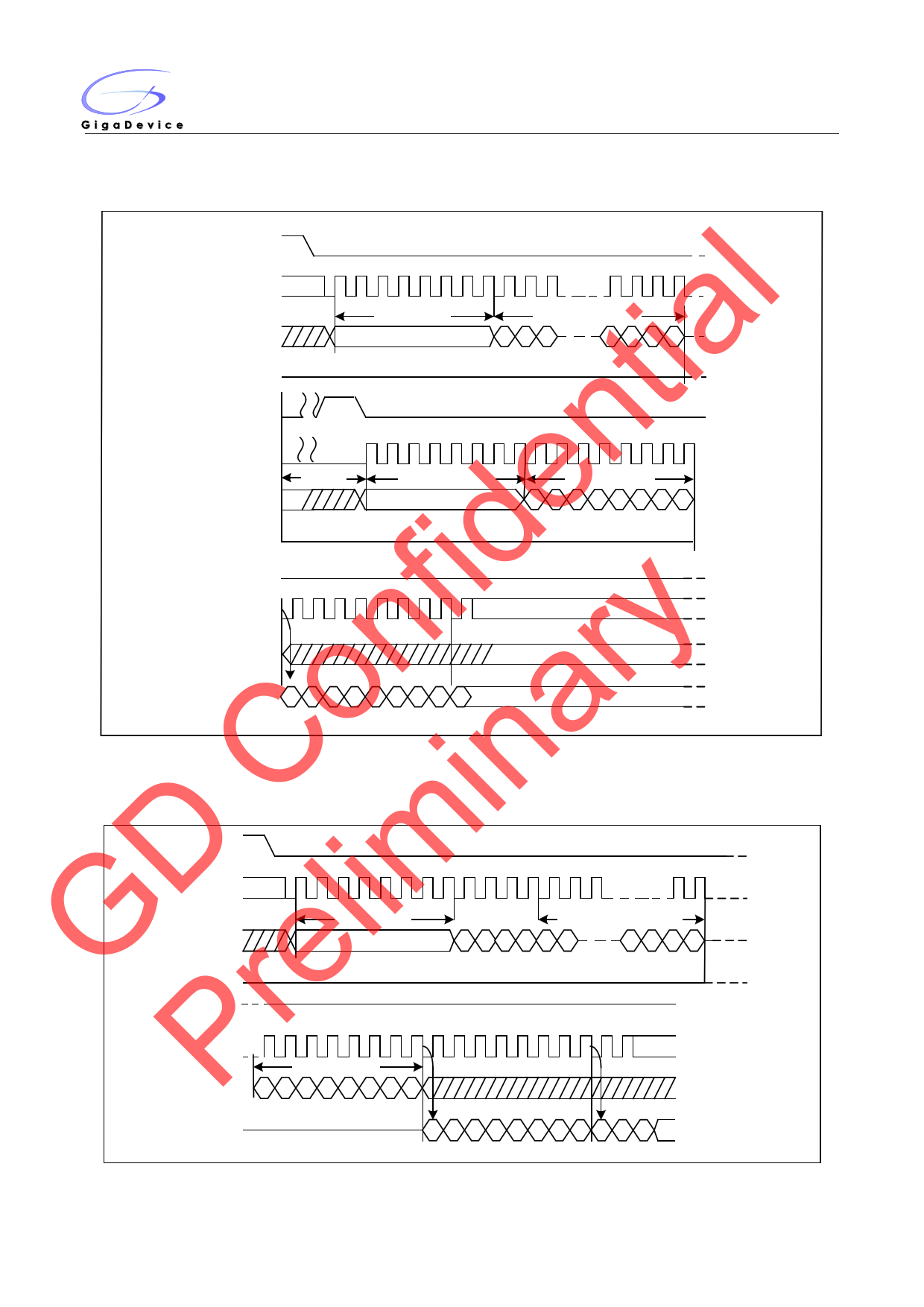
Read From Cache (03H or 0BH)
Figure10. Read From Cache Sequence Diagram
CS#
SCLK
0 1 2 3 4 5 6 7 8 9 10 11 12 13 14
22 23
Command
Wrap<3:0>
A11-0
SI
03H or 0BH
0 0 0 0 11 10
3210
SO
CS#
SCLK
SI
SO
High-Z
24 25 26 27 28 29 30 31 32 33 34 35 36 37 38 39
Dummy Byte
76543210
Data Out1
Data Out2
76543210765
MSB
MSB
11
11 Page | ||
| Páginas | Total 30 Páginas | |
| PDF Descargar | [ Datasheet GD5F1GQ4UAYIG.PDF ] | |
Hoja de datos destacado
| Número de pieza | Descripción | Fabricantes |
| GD5F1GQ4UAYIG | SPI (Serial Peripheral Interface) NAND Flash Memory | GigaDevice |
| Número de pieza | Descripción | Fabricantes |
| SLA6805M | High Voltage 3 phase Motor Driver IC. |
Sanken |
| SDC1742 | 12- and 14-Bit Hybrid Synchro / Resolver-to-Digital Converters. |
Analog Devices |
|
DataSheet.es es una pagina web que funciona como un repositorio de manuales o hoja de datos de muchos de los productos más populares, |
| DataSheet.es | 2020 | Privacy Policy | Contacto | Buscar |
