|
|
|
PDF M29W320ET Data sheet ( Hoja de datos )
| Número de pieza | M29W320ET | |
| Descripción | 32-Mbit 3V Supply Flash Memory | |
| Fabricantes | STMicroelectronics | |
| Logotipo | ||
Hay una vista previa y un enlace de descarga de M29W320ET (archivo pdf) en la parte inferior de esta página. Total 30 Páginas | ||
|
No Preview Available !
M29W320ET
M29W320EB
32 Mbit (4Mb x8 or 2Mb x16, Boot Block)
3V Supply Flash Memory
FEATURES SUMMARY
■ SUPPLY VOLTAGE
– VCC = 2.7V to 3.6V for Program, Erase
and Read
– VPP =12V for Fast Program (optional)
■ ACCESS TIMES: 70, 90ns
■ PROGRAMMING TIME
– 10µs per Byte/Word typical
– Double Word/ Quadruple Byte Program
■ MEMORY BLOCKS
– Memory Array: 63 Main Blocks
– 8 Parameter Blocks (Top or Bottom
Location)
■ ERASE SUSPEND and RESUME MODES
– Read and Program another Block during
Erase Suspend
■ UNLOCK BYPASS PROGRAM COMMAND
– Faster Production/Batch Programming
■ VPP/WP PIN for FAST PROGRAM and
WRITE PROTECT
■ TEMPORARY BLOCK UNPROTECTION
MODE
■ COMMON FLASH INTERFACE
– 64 bit Security Code
■ EXTENDED MEMORY BLOCK
– Extra block used as security block or to
store additional information
■ LOW POWER CONSUMPTION
– Standby and Automatic Standby
■ 100,000 PROGRAM/ERASE CYCLES per
BLOCK
■ ELECTRONIC SIGNATURE
– Manufacturer Code: 0020h
– Top Device Code M29W320ET: 2256h
– Bottom Device Code M29W320EB: 2257h
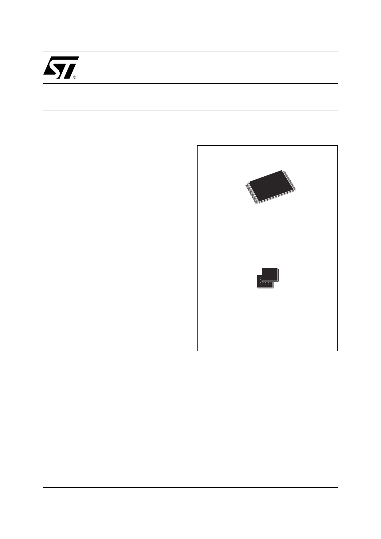
Figure 1. Packages
TSOP48 (N)
12 x 20mm
FBGA
TFBGA48 (ZE)
6 x 8mm
March 2005
1/46
1 page 
M29W320ET, M29W320EB
SUMMARY DESCRIPTION
The M29W320E is a 32 Mbit (4Mb x8 or 2Mb x16)
non-volatile memory that can be read, erased and
reprogrammed. These operations can be per-
formed using a single low voltage (2.7 to 3.6V)
supply. On power-up the memory defaults to its
Read mode.
The device features an asymmetrical block archi-
tecture. The M29W320E has an array of 8 param-
eter and 63 main blocks. M29W320ET locates the
Parameter Blocks at the top of the memory ad-
dress space while the M29W320EB locates the
Parameter Blocks starting from the bottom.
M29W320E has an extra 32 KWord (x16 mode) or
64 KByte (x8 mode) block, the Extended Block,
that can be accessed using a dedicated com-
mand. The Extended Block can be protected and
so is useful for storing security information. How-
ever the protection is irreversible, once protected
the protection cannot be undone.
Each block can be erased independently so it is
possible to preserve valid data while old data is
erased. The blocks can be protected to prevent
accidental Program or Erase commands from
modifying the memory. Program and Erase com-
mands are written to the Command Interface of
the memory. An on-chip Program/Erase Controller
simplifies the process of programming or erasing
the memory by taking care of all of the special op-
erations that are required to update the memory
contents. The end of a program or erase operation
can be detected and any error conditions identi-
fied. The command set required to control the
memory is consistent with JEDEC standards.
Chip Enable, Output Enable and Write Enable sig-
nals control the bus operation of the memory.
They allow simple connection to most micropro-
cessors, often without additional logic.
The memory is offered in TSOP48 (12x20mm), and
TFBGA48 (6x8mm, 0.8mm pitch) packages. The
memory is supplied with all the bits erased (set to
’1’).
Figure 2. Logic Diagram
VCC VPP/WP
21
A0-A20
15
DQ0-DQ14
W DQ15A–1
M29W320ET
E M29W320EB BYTE
G RB
RP
VSS
AI09346
Table 1. Signal Names
A0-A20
Address Inputs
DQ0-DQ7 Data Inputs/Outputs
DQ8-DQ14 Data Inputs/Outputs
DQ15A–1 Data Input/Output or Address Input
E Chip Enable
G Output Enable
W Write Enable
RP Reset/Block Temporary Unprotect
RB Ready/Busy Output
BYTE
Byte/Word Organization Select
VCC Supply Voltage
VPP/WP
VPP/Write Protect
VSS Ground
NC Not Connected Internally
5/46
5 Page 
M29W320ET, M29W320EB
Ready/Busy is Low, VOL. Ready/Busy is high-im-
pedance during Read mode, Auto Select mode
and Erase Suspend mode.
After a Hardware Reset, Bus Read and Bus Write
operations cannot begin until Ready/Busy be-
comes high-impedance. See Table 16. and Figure
16., Reset/Block Temporary Unprotect AC Wave-
forms.
The use of an open-drain output allows the Ready/
Busy pins from several memories to be connected
to a single pull-up resistor. A Low will then indicate
that one, or more, of the memories is busy.
Byte/Word Organization Select (BYTE). The
Byte/Word Organization Select pin is used to
switch between the x8 and x16 Bus modes of the
memory. When Byte/Word Organization Select is
Low, VIL, the memory is in x8 mode, when it is
High, VIH, the memory is in x16 mode.
VCC Supply Voltage (2.7V to 3.6V). VCC pro-
vides the power supply for all operations (Read,
Program and Erase).
The Command Interface is disabled when the VCC
Supply Voltage is less than the Lockout Voltage,
VLKO. This prevents Bus Write operations from ac-
cidentally damaging the data during power up,
power down and power surges. If the Program/
Erase Controller is programming or erasing during
this time then the operation aborts and the memo-
ry contents being altered will be invalid.
A 0.1µF capacitor should be connected between
the VCC Supply Voltage pin and the VSS Ground
pin to decouple the current surges from the power
supply. The PCB track widths must be sufficient to
carry the currents required during Program and
Erase operations, ICC3.
VSS Ground. VSS is the reference for all voltage
measurements. The device features two VSS pins
which must be both connected to the system
ground.
11/46
11 Page | ||
| Páginas | Total 30 Páginas | |
| PDF Descargar | [ Datasheet M29W320ET.PDF ] | |
Hoja de datos destacado
| Número de pieza | Descripción | Fabricantes |
| M29W320E | 32-Mbit 3V Supply Flash Memory | ST Microelectronics |
| M29W320EB | 32-Mbit 3V supply Flash memory | Numonyx |
| M29W320EB | 32-Mbit 3V Supply Flash Memory | STMicroelectronics |
| M29W320ET | 32-Mbit 3V supply Flash memory | Numonyx |
| Número de pieza | Descripción | Fabricantes |
| SLA6805M | High Voltage 3 phase Motor Driver IC. |
Sanken |
| SDC1742 | 12- and 14-Bit Hybrid Synchro / Resolver-to-Digital Converters. |
Analog Devices |
|
DataSheet.es es una pagina web que funciona como un repositorio de manuales o hoja de datos de muchos de los productos más populares, |
| DataSheet.es | 2020 | Privacy Policy | Contacto | Buscar |