|
|
|
PDF NVD4808N Data sheet ( Hoja de datos )
| Número de pieza | NVD4808N | |
| Descripción | Power MOSFET ( Transistor ) | |
| Fabricantes | ON Semiconductor | |
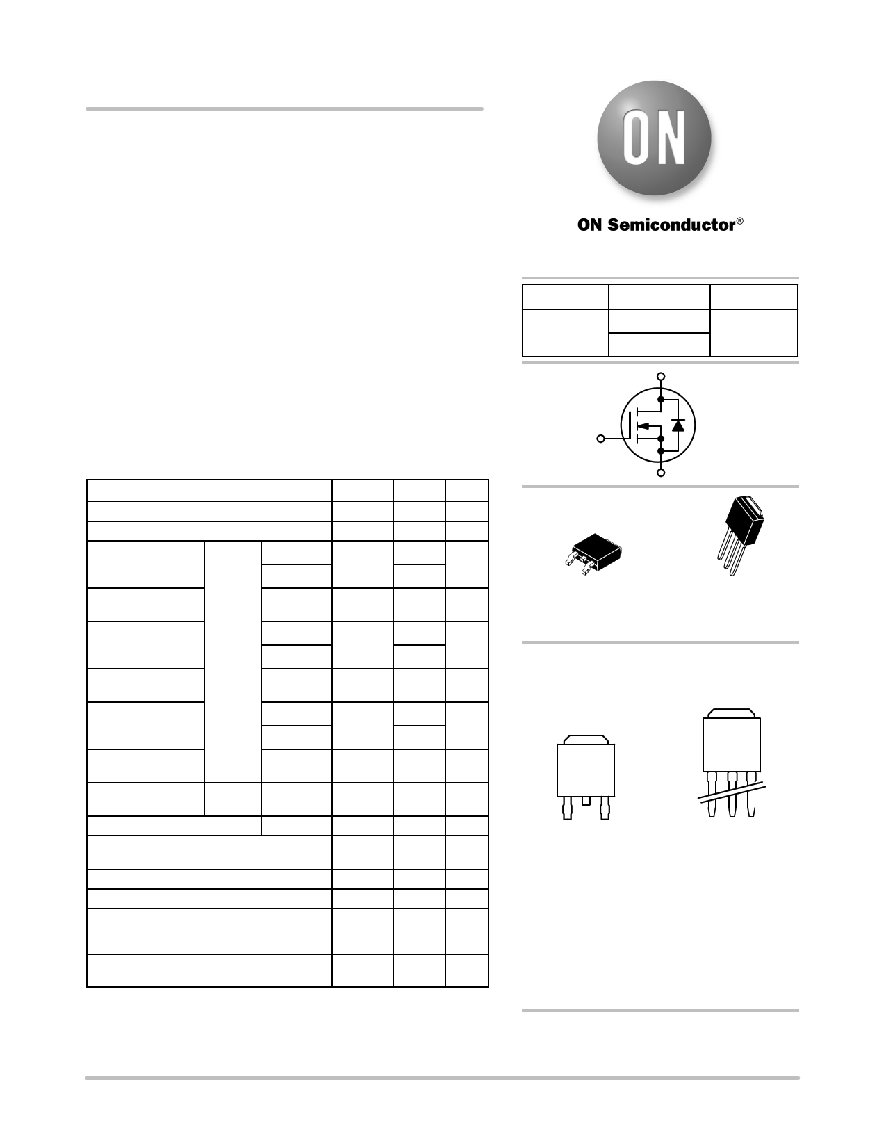
| Logotipo | ||
Hay una vista previa y un enlace de descarga de NVD4808N (archivo pdf) en la parte inferior de esta página. Total 8 Páginas | ||
|
No Preview Available !
NTD4808N, NVD4808N
Power MOSFET
30 V, 63 A, Single N−Channel, DPAK/IPAK
Features
• Low RDS(on) to Minimize Conduction Losses
• Low Capacitance to Minimize Driver Losses
• Optimized Gate Charge to Minimize Switching Losses
• NVD Prefix for Automotive and Other Applications Requiring
Unique Site and Control Change Requirements; AEC−Q101
Qualified and PPAP Capable
• These are Pb−Free Devices
Applications
• CPU Power Delivery
• DC−DC Converters
• Low Side Switching
MAXIMUM RATINGS (TJ = 25°C unless otherwise stated)
Parameter
Symbol Value Unit
Drain−to−Source Voltage
Gate−to−Source Voltage
Continuous Drain
Current RqJA
(Note 1)
TA = 25°C
TA = 85°C
VDSS
VGS
ID
30
±20
13.8
10.7
V
V
A
Power Dissipation
RqJA (Note 1)
Continuous Drain
Current RqJA
(Note 2)
Power Dissipation
RqJA (Note 2)
Continuous Drain
Current RqJC
(Note 1)
TA = 25°C
Steady
State
TA = 25°C
TA = 85°C
TA = 25°C
TC = 25°C
TC = 85°C
PD
ID
PD
ID
2.63 W
10 A
7.8
1.4 W
63 A
49
Power Dissipation
RqJC (Note 1)
Pulsed Drain
Current
TC = 25°C
tp=10ms TA = 25°C
PD
IDM
54.6 W
126 A
Current Limited by Package
TA = 25°C
Operating Junction and Storage
Temperature
Source Current (Body Diode)
Drain to Source dV/dt
IDmaxPkg
TJ,
TSTG
IS
dV/dt
45
−55 to
+175
45
6
A
°C
A
V/ns
Single Pulse Drain−to−Source Avalanche
Energy (VDD = 24 V, VGS = 10 V,
IL = 17 Apk, L = 1.0 mH, RG = 25 W)
Lead Temperature for Soldering Purposes
(1/8” from case for 10 s)
EAS
144.5 mJ
TL 260 °C
Stresses exceeding those listed in the Maximum Ratings table may damage the
device. If any of these limits are exceeded, device functionality should not be
assumed, damage may occur and reliability may be affected.
© Semiconductor Components Industries, LLC, 2014
September, 2014 − Rev. 8
1
http://onsemi.com
V(BR)DSS
30 V
RDS(ON) MAX
8.0 mW @ 10 V
12.4 mW @ 4.5 V
D
ID MAX
63 A
N−Channel
G
S
4
4
12
3
DPAK
CASE 369AA
STYLE 2
1
2
3
IPAK
CASE 369D
STYLE 2
MARKING DIAGRAMS
& PIN ASSIGNMENTS
4
Drain
4
Drain
2
1 Drain 3
Gate Source
1 23
Gate Drain Source
A = Assembly Location*
Y = Year
WW = Work Week
4808N = Device Code
G = Pb−Free Package
* The Assembly Location code (A) is front side
optional. In cases where the Assembly Location is
stamped in the package, the front side assembly
code may be blank.
ORDERING INFORMATION
See detailed ordering and shipping information on page 6 of
this data sheet.
Publication Order Number:
NTD4808N/D
1 page 
NTD4808N, NVD4808N
TYPICAL PERFORMANCE CURVES
2000
1500
TJ = 25°C
Ciss
1000
500 Coss
0 Crss
0 5 10 15 20 25
GATE−TO−SOURCE OR DRAIN−TO−SOURCE VOLTAGE (VOLTS)
Figure 7. Capacitance Variation
100
tr
td(off)
10
td(on)
tf
1
1
VDD = 15 V
ID = 30 A
VGS = 11.5 V
10 100
RG, GATE RESISTANCE (OHMS)
Figure 9. Resistive Switching Time
Variation vs. Gate Resistance
1000
VGS = 20 V
SINGLE PULSE
TC = 25°C
100
10 ms
100 ms
10 1 ms
1
0.1
RDS(on) LIMIT
THERMAL LIMIT
PACKAGE LIMIT
10 ms
dc
1 10 100
VDS, DRAIN−TO−SOURCE VOLTAGE (VOLTS)
Figure 11. Maximum Rated Forward Biased
Safe Operating Area
5
4 Q1
QT
Q2
3
2
VDD = 15 V
1 VGS = 4.5 V
ID = 30 A
0 TJ = 25°C
0 1 2 3 4 5 6 7 8 9 10 11 12
QG, TOTAL GATE CHARGE (nC)
Figure 8. Gate−To−Source and Drain−To−Source
Voltage vs. Total Charge
30
VGS = 0 V
25 TJ = 25°C
20
15
10
5
0
0.5 0.6 0.7 0.8 0.9 1.0
VSD, SOURCE−TO−DRAIN VOLTAGE (VOLTS)
Figure 10. Diode Forward Voltage vs. Current
100
90 ID = 17 A
80
70
60
50
40
30
20
10
0
50 75 100 125 150 175
TJ, JUNCTION TEMPERATURE (°C)
Figure 12. Maximum Avalanche Energy vs.
Starting Junction Temperature
http://onsemi.com
5
5 Page | ||
| Páginas | Total 8 Páginas | |
| PDF Descargar | [ Datasheet NVD4808N.PDF ] | |
Hoja de datos destacado
| Número de pieza | Descripción | Fabricantes |
| NVD4808N | Power MOSFET ( Transistor ) | ON Semiconductor |
| Número de pieza | Descripción | Fabricantes |
| SLA6805M | High Voltage 3 phase Motor Driver IC. |
Sanken |
| SDC1742 | 12- and 14-Bit Hybrid Synchro / Resolver-to-Digital Converters. |
Analog Devices |
|
DataSheet.es es una pagina web que funciona como un repositorio de manuales o hoja de datos de muchos de los productos más populares, |
| DataSheet.es | 2020 | Privacy Policy | Contacto | Buscar |