|
|
|
PDF NCV8154 Data sheet ( Hoja de datos )
| Número de pieza | NCV8154 | |
| Descripción | Dual Input Voltage Regulator | |
| Fabricantes | ON Semiconductor | |
| Logotipo | ||
Hay una vista previa y un enlace de descarga de NCV8154 (archivo pdf) en la parte inferior de esta página. Total 16 Páginas | ||
|
No Preview Available !
NCV8154
Dual 300 mA, Low IQ, Low
Dropout, Dual Input Voltage
Regulator
The NCV8154 is 300 mA, Dual Output Linear Voltage Regulator
that offers two independent input pins and provides a very stable and
accurate voltage with ultra low noise and very high Power Supply
Rejection Ratio (PSRR) suitable for RF applications. The NCV8154 is
suitable for powering RF blocks of automotive infotainment systems
and other power sensitive device. Due to low power consumption the
NCV8154 offers high efficiency and low thermal dissipation.
Features
• Operating Input Voltage Range: 1.9 V to 5.25 V
• Two Independent Input Voltage Pins
• Two Independent Output Voltage (for detail please refer to Ordering
Information)
• Low IQ of typ. 55 mA per Channel
• High PSRR: 75 dB at 1 kHz
• Very Low Dropout: 140 mV Typical at 300 mA
• Thermal Shutdown and Current Limit Protections
• Stable with a 1 mF Ceramic Output Capacitor
• Available in DFN10 3 × 3 mm Package
• Active Output Discharge for Fast Output Turn-Off
• NCV Prefix for Automotive and Other Applications Requiring
Unique Site and Control Change Requirements; AEC−Q100
Qualified and PPAP Capable
• These are Pb-free Devices
Typical Applications
• Applications Requiring Wettable Flanks for Enhanced Visual
Inspection
• Wireless LAN, Bluetooth®, ZigBee® Interfaces
• Automotive Infotainment Systems
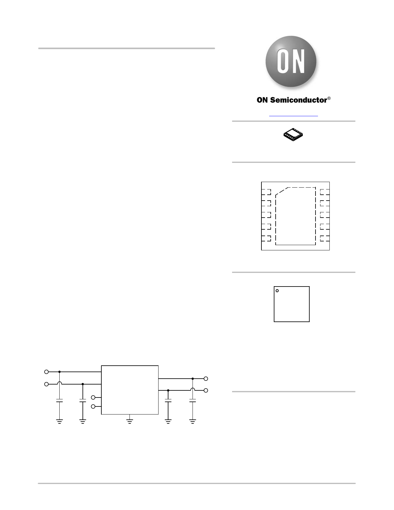
VIN1
VIN2
CIN1
1 mF
CIN2
1 mF
NCV8154
IN1
OUT1
IN2
OUT2
EN1
EN2
GND
VOUT1
VOUT2
COUT2
1 mF
COUT1
1 mF
Figure 1. Typical Application Schematic
www.onsemi.com
DFN10, 3x3
CASE 485C
PIN CONNECTIONS
GND 1
OUT1 2
OUT2 3
GND 4
N/C 5
10 EN1
9 IN1
EP 8 IN2
7 EN2
6 N/C
DFN10
(Top View)
MARKING DIAGRAM
NCV8154x
VVVVV
ALYWG
G
x = NCV8154N − Non wettable flank
= NCV8154W − Wettable flank
VVVVV = Voltage Option
A = Assembly Location
L = Wafer Lot
Y = Year
W = Work Week
G = Pb−Free Package
(Note: Microdot may be in either location)
ORDERING INFORMATION
See detailed ordering, marking and shipping information on
page 15 of this data sheet.
© Semiconductor Components Industries, LLC, 2015
April, 2015 − Rev. 3
1
Publication Order Number:
NCV8154/D
1 page 
NCV8154
TYPICAL CHARACTERISTICS
1.85
1.84
1.83
1.82
1.81
1.80
1.79
IOUT = 1 mA
IOUT = 300 mA
1.78
1.77
1.76
1.75
−40
−20
0
VIN = 2.8 V
VOUT = 1.8 V
CIN = COUT = 1 mF
20 40 60 80 100 120 140
TJ, JUNCTION TEMPERATURE (°C)
Figure 3. Output Voltage vs. Temperature
VOUT = 1.8 V
3.35
3.34
3.33
3.32
3.31
3.30
IOUT = 1 mA
IOUT = 300 mA
3.29
3.28
3.27
3.26
3.25
−40
−20
0
VIN = 4.3 V
VOUT = 3.3 V
CIN = COUT = 1 mF
20 40 60 80 100 120 140
TJ, JUNCTION TEMPERATURE (°C)
Figure 4. Output Voltage vs. Temperature
VOUT = 3.3 V
600
540
480 TJ = 125°C
420 TJ = 25°C
360 TJ = −40°C
300
240
180
120 VIN = 4.3 V
60 VOUT = 3.3 V
CIN = COUT = 1 mF
0
0 60 120 180 240 300
IOUT, OUTPUT CURRENT (mA)
Figure 5. Ground Current vs. Output Current
60
54 TJ = 125°C
48
TJ = −40°C
52
TJ = 25°C
36
30
24
18
12 VIN = 4.3 V
6 VOUT = 3.3 V
0 CIN = COUT = 1 mF
0 0.5 1 1.5 2 2.5 3 3.5 4 4.5 5 5.5
VIN, INPUT VOLTAGE (V)
Figure 6. Quiescent Current vs. Input Voltage
60
58
56
54
52
50
48
46
44
42
40
−40
−20
0
VIN = 4.3 V
VOUT = 3.3 V
CIN = COUT = 1 mF
20 40 60 80 100 120 140
TJ, JUNCTION TEMPERATURE (°C)
Figure 7. Quiescent Current vs. Temperature
0.1
0.08
0.06
0.04
0.02
0
−0.02
−0.04
−0.06
0.08
−0.1
−40
−20
0
VIN = 2.8 V
VOUT = 1.8 V
CIN = COUT = 1 mF
20 40 60 80 100 120 140
TJ, JUNCTION TEMPERATURE (°C)
Figure 8. Line Regulation vs. Temperature
VOUT = 1.8 V
www.onsemi.com
5
5 Page 
NCV8154
TYPICAL CHARACTERISTICS
IOUT1
VOUT1
VIN = VOUT + 1 V
tRISE = 1 ms
VOUT1 = 3.3 V
VOUT2 = 1.8 V
IOUT2 = 10 mA
COUT1 = 1 mF
COUT2 = 1 mF
VOUT2
4 ms/div
Figure 36. Load Transient Response − 1.8 V −
Rising Edge, IOUT1 = 100 mA to 300 mA
IOUT1
tFALL = 1 ms
VOUT1
VOUT2
VIN = VOUT + 1 V
VOUT1 = 3.3 V
VOUT2 = 1.8 V
IOUT2 = 10 mA
COUT1 = 1 mF
COUT2 = 1 mF
100 ms/div
Figure 37. Load Transient Response − 1.8 V −
Falling Edge, IOUT1 = 300 mA to 100 mA
IOUT1
VOUT1
VOUT2
tRISE = 500 ns
VIN = VOUT + 1 V
VOUT1 = 3.3 V
VOUT2 = 1.8 V
IOUT2 = 10 mA
COUT1 = 1 mF
COUT2 = 1 mF
4 ms/div
Figure 38. Load Transient Response − 1.8 V −
Rising Edge, IOUT1 = 1 mA to 300 mA
IOUT1
tFALL = 500 ns
VOUT1
VOUT2
VIN = VOUT + 1 V
VOUT1 = 3.3 V
VOUT2 = 1.8 V
IOUT2 = 10 mA
COUT1 = 1 mF
COUT2 = 1 mF
10 ms/div
Figure 39. Load Transient Response − 1.8 V −
Falling Edge, IOUT1 = 300 mA to 1 mA
IOUT1
VOUT1
VOUT2
tRISE = 500 ns
VIN = VOUT + 1 V
VOUT1 = 3.3 V
VOUT2 = 1.8 V
IOUT2 = 10 mA
COUT1 = 1 mF
COUT2 = 1 mF
4 ms/div
Figure 40. Load Transient Response − 1.8 V −
Rising Edge, IOUT = 50 mA to 300 mA
IOUT1
tFALL = 500 ns
VOUT1
VOUT2
VIN = VOUT + 1 V
VOUT1 = 3.3 V
VOUT2 = 1.8 V
IOUT2 = 10 mA
COUT1 = 1 mF
COUT2 = 1 mF
4 ms/div
Figure 41. Load Transient Response − Falling
Edge, IOUT = 300 mA to 50 mA
www.onsemi.com
11
11 Page | ||
| Páginas | Total 16 Páginas | |
| PDF Descargar | [ Datasheet NCV8154.PDF ] | |
Hoja de datos destacado
| Número de pieza | Descripción | Fabricantes |
| NCV8154 | Dual Input Voltage Regulator | ON Semiconductor |
| Número de pieza | Descripción | Fabricantes |
| SLA6805M | High Voltage 3 phase Motor Driver IC. |
Sanken |
| SDC1742 | 12- and 14-Bit Hybrid Synchro / Resolver-to-Digital Converters. |
Analog Devices |
|
DataSheet.es es una pagina web que funciona como un repositorio de manuales o hoja de datos de muchos de los productos más populares, |
| DataSheet.es | 2020 | Privacy Policy | Contacto | Buscar |