|
|
|
PDF NCV4266 Data sheet ( Hoja de datos )
| Número de pieza | NCV4266 | |
| Descripción | 150mA Low-Dropout Voltage Regulator | |
| Fabricantes | ON Semiconductor | |
| Logotipo | ||
Hay una vista previa y un enlace de descarga de NCV4266 (archivo pdf) en la parte inferior de esta página. Total 11 Páginas | ||
|
No Preview Available !
NCV4266
150 mA Low-Dropout
Voltage Regulator with
Enable
The NCV4266 is a 150 mA output current integrated low dropout
regulator family designed for use in harsh automotive environments.
It includes wide operating temperature and input voltage ranges. The
device is offered with fixed voltage versions of 3.3 V and 5.0 V
available in 2% output voltage accuracy. It has a high peak input
voltage tolerance and reverse input voltage protection. It also
provides overcurrent protection, overtemperature protection and
enable function for control of the state of the output voltage. The
NCV4266 is available in SOT−223 surface mount package. The
output is stable over a wide output capacitance and ESR range. The
NCV4266 has improved startup behavior during input voltage
transients.
Features
• 3.3 V and 5.0 V Output Voltage
• 150 mA Output Current
• 500 mV (max) Dropout Voltage
• Enable Input
• Very Low Current Consumption
• Fault Protection
♦ +45 V Peak Transient Voltage
♦ −42 V Reverse Voltage
♦ Short Circuit
♦ Thermal Overload
• NCV Prefix for Automotive and Other Applications Requiring
Unique Site and Control Change Requirements; AEC−Q100
Qualified and PPAP Capable
• These are Pb−Free Devices
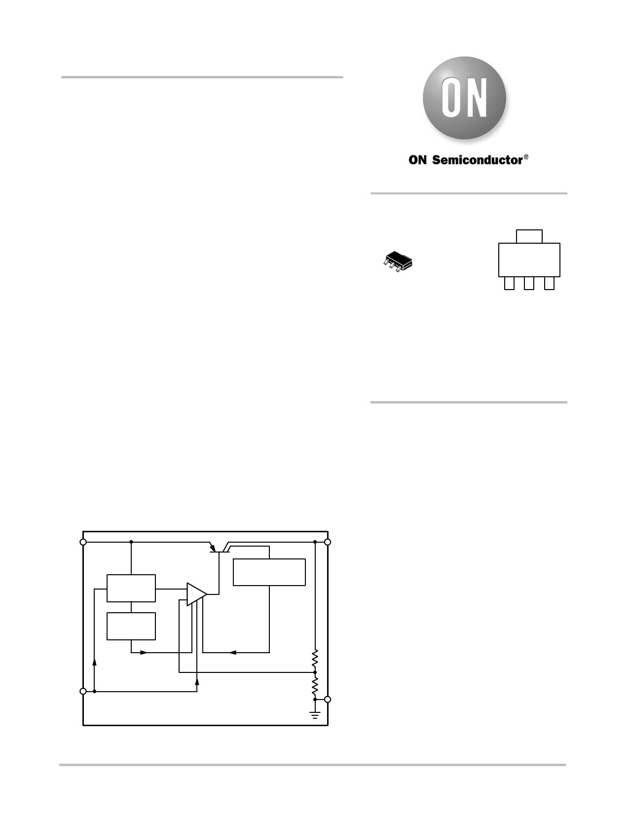
IQ
Bandgap
Reference
Thermal
Shutdown
Error
Amplifier
−
+
Current Limit and
Saturation Sense
http://onsemi.com
MARKING
DIAGRAM
SOT−223
(TO−261)
ST SUFFIX
CASE 318E
AYW
4266xG
G
1
A = Assembly Location
Y = Year
W = Work Week
x = Voltage Option
3.3 V (x = 3)
5.0 V (x = 5)
G = Pb−Free Package
(*Note: Microdot may be in either location)
ORDERING INFORMATION
See detailed ordering and shipping information in the ordering
information section on page 10 of this data sheet.
EN
Figure 1. Block Diagram
© Semiconductor Components Industries, LLC, 2012
June, 2012 − Rev. 2
GND
1
Publication Order Number:
NCV4266/D
1 page 
NCV4266
TYPICAL PERFORMANCE CHARACTERISTICS
6
TJ = 25°C
5 RL = 33 W
4
3
2
1
0
024 68
VI, INPUT VOLTAGE (V)
Figure 8. Output Voltage vs. Input Voltage,
5.0 V Version
10
6.0
4.0
2.0
0
−2.0
−4.0
−6.0
−8.0
−10
−50
−25
0
TJ = 25°C
RL = 6.8 kW
25 50
VI, INPUT VOLTAGE (V)
Figure 10. Input Current vs. Input Voltage,
5.0 V Version
6
TJ = 25°C
5 RL = 22 W
4
3
2
1
0
024 68
VI, INPUT VOLTAGE (V)
Figure 9. Output Voltage vs. Input Voltage,
3.3 V Version
10
1
0
−1
−2
−3
−4
−5
−6
TJ = 25°C
RL = 6.8 kW
−7
−50 −25 0 25 50
VI, INPUT VOLTAGE (V)
Figure 11. Input Current vs. Input Voltage,
3.3 V Version
300
250
200 TJ = 125°C
150
TJ = 25°C
100
50
0
0 25 50 75 100 125
IQ, OUTPUT CURRENT (mA)
Figure 12. Dropout Voltage vs. Output Current
(5.0 V Version only)
150
400
350
TJ = 25°C
VQ = 0 V
300
250
200
150
100
50
0
0 5 10 15 20 25 30 35
VI, INPUT VOLTAGE (V)
Figure 13. Maximum Output Current vs.
Input Voltage
40
http://onsemi.com
5
5 Page 
NCV4266
PACKAGE DIMENSIONS
D
b1
4
HE
1 23
e1 e
0.08 (0003)
A1
E
b
A
SOT−223 (TO−261)
CASE 318E−04
ISSUE N
q
L
C
L1
NOTES:
1. DIMENSIONING AND TOLERANCING PER ASME Y14.5M,
1994.
2. CONTROLLING DIMENSION: INCH.
MILLIMETERS
INCHES
DIM MIN
NOM MAX
MIN NOM
A 1.50
1.63
1.75
0.060 0.064
A1 0.02
0.06
0.10
0.001 0.002
b 0.60 0.75 0.89 0.024 0.030
b1 2.90
3.06
3.20
0.115 0.121
c 0.24 0.29 0.35 0.009 0.012
D 6.30
6.50
6.70
0.249 0.256
E 3.30 3.50 3.70 0.130 0.138
e 2.20 2.30 2.40 0.087 0.091
e1 0.85
0.94
1.05
0.033 0.037
L 0.20
−−−
−−−
0.008
−−−
L1 1.50
1.75
2.00
0.060 0.069
H E 6.70
7.00
7.30
0.264 0.276
q 0° − 10° 0° −
MAX
0.068
0.004
0.035
0.126
0.014
0.263
0.145
0.094
0.041
−−−
0.078
0.287
10°
SOLDERING FOOTPRINT
3.8
0.15
2.0
0.079
2.3
0.091
2.3
0.091
6.3
0.248
2.0
0.079
1.5
0.059
ǒ ǓSCALE 6:1
mm
inches
ON Semiconductor and
are registered trademarks of Semiconductor Components Industries, LLC (SCILLC). SCILLC owns the rights to a number of patents, trademarks,
copyrights, trade secrets, and other intellectual property. A listing of SCILLC’s product/patent coverage may be accessed at www.onsemi.com/site/pdf/Patent−Marking.pdf . SCILLC
reserves the right to make changes without further notice to any products herein. SCILLC makes no warranty, representation or guarantee regarding the suitability of its products
for any particular purpose, nor does SCILLC assume any liability arising out of the application or use of any product or circuit, and specifically disclaims any and all liability, including
without limitation special, consequential or incidental damages. “Typical” parameters which may be provided in SCILLC data sheets and/or specifications can and do vary in different
applications and actual performance may vary over time. All operating parameters, including “Typicals” must be validated for each customer application by customer’s technical
experts. SCILLC does not convey any license under its patent rights nor the rights of others. SCILLC products are not designed, intended, or authorized for use as components
in systems intended for surgical implant into the body, or other applications intended to support or sustain life, or for any other application in which the failure of the SCILLC product
could create a situation where personal injury or death may occur. Should Buyer purchase or use SCILLC products for any such unintended or unauthorized application, Buyer shall
indemnify and hold SCILLC and its officers, employees, subsidiaries, affiliates, and distributors harmless against all claims, costs, damages, and expenses, and reasonable attorney
fees arising out of, directly or indirectly, any claim of personal injury or death associated with such unintended or unauthorized use, even if such claim alleges that SCILLC was
negligent regarding the design or manufacture of the part. SCILLC is an Equal Opportunity/Affirmative Action Employer. This literature is subject to all applicable copyright laws
and is not for resale in any manner.
PUBLICATION ORDERING INFORMATION
LITERATURE FULFILLMENT:
Literature Distribution Center for ON Semiconductor
P.O. Box 5163, Denver, Colorado 80217 USA
Phone: 303−675−2175 or 800−344−3860 Toll Free USA/Canada
Fax: 303−675−2176 or 800−344−3867 Toll Free USA/Canada
Email: [email protected]
N. American Technical Support: 800−282−9855 Toll Free
USA/Canada
Europe, Middle East and Africa Technical Support:
Phone: 421 33 790 2910
Japan Customer Focus Center
Phone: 81−3−5817−1050
ON Semiconductor Website: www.onsemi.com
Order Literature: http://www.onsemi.com/orderlit
For additional information, please contact your loca
Sales Representative
http://onsemi.com
11
NCV4266/D
11 Page | ||
| Páginas | Total 11 Páginas | |
| PDF Descargar | [ Datasheet NCV4266.PDF ] | |
Hoja de datos destacado
| Número de pieza | Descripción | Fabricantes |
| NCV4263-2C | 200 mA LDO Regulator | ON Semiconductor |
| NCV4264 | Low Dropout Linear Regulator | ON Semiconductor |
| NCV4264-2 | Low Dropout Linear Regulator | ON Semiconductor |
| NCV4264-2C | Low Dropout Linear Regulator | ON Semiconductor |
| Número de pieza | Descripción | Fabricantes |
| SLA6805M | High Voltage 3 phase Motor Driver IC. |
Sanken |
| SDC1742 | 12- and 14-Bit Hybrid Synchro / Resolver-to-Digital Converters. |
Analog Devices |
|
DataSheet.es es una pagina web que funciona como un repositorio de manuales o hoja de datos de muchos de los productos más populares, |
| DataSheet.es | 2020 | Privacy Policy | Contacto | Buscar |