|
|
|
PDF NCV8716 Data sheet ( Hoja de datos )
| Número de pieza | NCV8716 | |
| Descripción | Wide Input Voltage Low Dropout Regulator | |
| Fabricantes | ON Semiconductor | |
| Logotipo | ||
Hay una vista previa y un enlace de descarga de NCV8716 (archivo pdf) en la parte inferior de esta página. Total 16 Páginas | ||
|
No Preview Available !
NCV8716
80 mA Ultra-Low Iq, Wide
Input Voltage Low Dropout
Regulator
The NCV8716 is 80 mA LDO Linear Voltage Regulator. It is a very
stable and accurate device with ultra−low ground current consumption
(4.7 mA over the full output load range) and a wide input voltage range
(up to 24 V). The regulator incorporates several protection features
such as Thermal Shutdown and Current Limiting.
Features
• Operating Input Voltage Range: 2.5 V to 24 V
• Fixed Voltage Options Available:
1.5 V to 5.0 V
• Ultra Low Quiescent Current: Max. 4.7 mA over Temperature
• ±2% Accuracy over Full Load, Line and Temperature Variations
• PSRR: 60 dB at 100 kHz
• Noise: 200 mVRMS from 200 Hz to 100 kHz
• Thermal Shutdown and Current Limit Protection
• Available in wDFN6, 2x2x0.8 mm Package
• This is a Pb−Free Device
Typical Applications
• Portable Equipment
• Communication Systems
www.onsemi.com
WDFN6
CASE 511BR
MARKING
DIAGRAMS
1
XX M
XX = Specific Device Code
M = Date Code
PIN CONNECTIONS
16
2 EXP
3
5
4
WDFN6 2x2 mm
(Top View)
ORDERING INFORMATION
See detailed ordering, marking and shipping information on
page 15 of this data sheet.
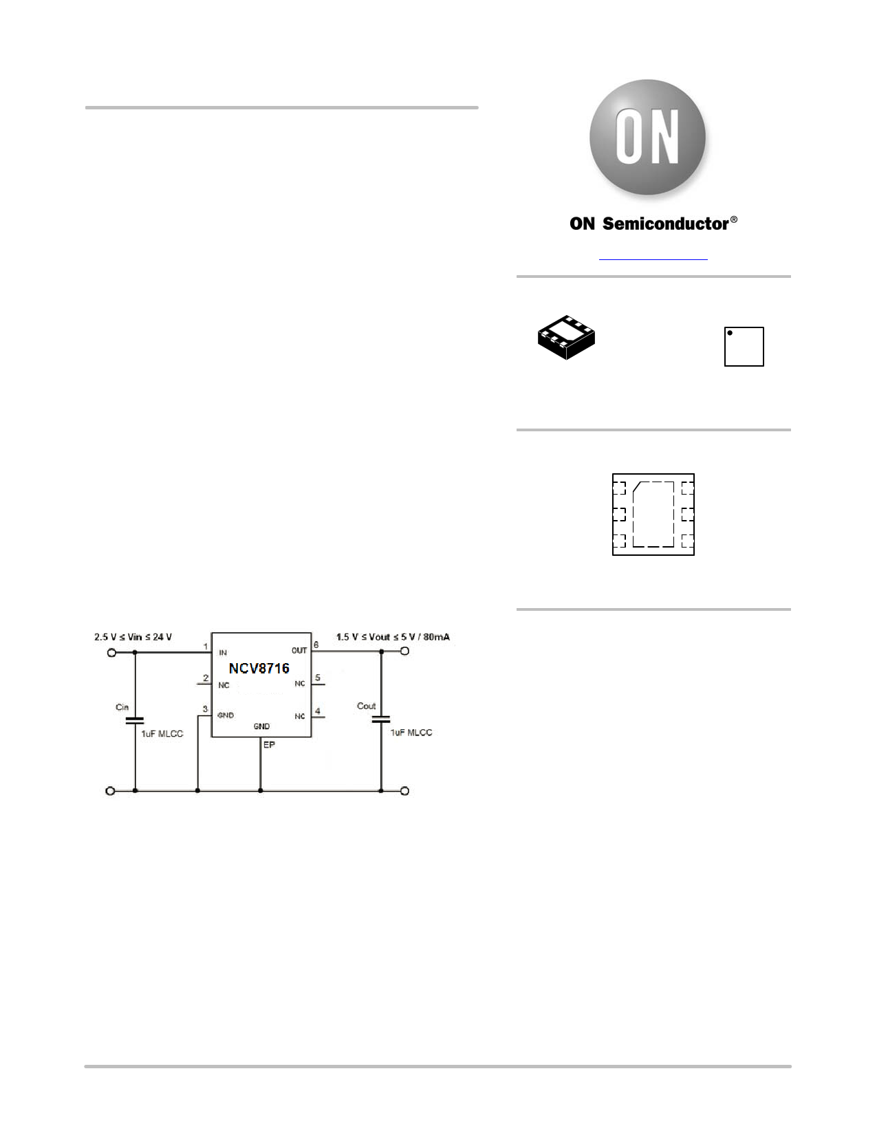
Figure 1. Typical Application Schematic
© Semiconductor Components Industries, LLC, 2015
April, 2015 − Rev. 3
1
Publication Order Number:
NCV8716/D
1 page 
NCV8716
Table 6. ELECTRICAL CHARACTERISTICS Voltage version 2.5 V
−40°C ≤ TJ ≤ 125°C; VIN = 3.5 V; IOUT = 1 mA, CIN = COUT = 1.0 mF, unless otherwise noted. Typical values are at TJ = +25°C. (Note 13)
Parameter
Test Conditions
Symbol Min Typ Max Unit
Operating Input Voltage
Output Voltage Accuracy
Line Regulation
Load Regulation
Dropout voltage (Note 11)
Maximum Output Current
Ground current
Power Supply Rejection Ratio
Output Noise Voltage
IOUT = 80 mA
VIN 3.5
24 V
3.5 V < VIN < 24 V, 0 < IOUT < 80 mA
VOUT 2.45 2.5 2.55
V
VOUT + 1 V ≤ VIN ≤ 24 V, IOUT = 1mA
RegLINE
15 20 mV
IOUT = 0 mA to 80 mA
RegLOAD
15 20 mV
VDO = VIN – (VOUT(NOM) – 125 mV)
IOUT = 80 mA
VDO
640 mV
400
(Note 14)
IOUT
110
mA
0 < IOUT < 80 mA, VIN = 24 V
IGND
3.4 5.8 mA
VIN = 3.5 V, VOUT = 2.5 V
VPP = 200 mV modulation
IOUT = 1 mA, COUT = 10 mF
f = 100 kHz
PSRR
60
dB
VOUT = 2.5 V, IOUT = 80 mA
f = 200 Hz to 100 kHz
VN
160 mVrms
Thermal Shutdown Temperature (Note 12) Temperature increasing from TJ = +25°C
TSD
155 °C
Thermal Shutdown Hysteresis (Note 12)
Temperature falling from TSD
TSDH − 25 − °C
Product parametric performance is indicated in the Electrical Characteristics for the listed test conditions, unless otherwise noted. Product
performance may not be indicated by the Electrical Characteristics if operated under different conditions.
11. Characterized when VOUT falls 125 mV below the regulated voltage and only for devices with VOUT = 2.5 V
12. Guaranteed by design and characterization.
13. Performance guaranteed over the indicated operating temperature range by design and/or characterization production tested at TJ = TA =
25°C. Low duty cycle pulse techniques are used during testing to maintain the junction temperature as close to ambient as possible.
14. Respect SOA
www.onsemi.com
5
5 Page 
NCV8716
TYPICAL CHARACTERISTICS
30 40
25
TA = 25°C
CIN = COUT = 1 mF
35
30
TA = 25°C
CIN = COUT = 1 mF
20
25
15 20
10
5 IOUT = 80 mA
IOUT = 0
0
0 5 10 15 20 25
INPUT VOLTAGE (V)
Figure 15. NCV8716x25xxx Ground Current vs.
Input Voltage
30
25 TA = 25°C
CIN = COUT = 1 mF
20
15
15
10
5
0
0
IOUT = 80 mA
5 10 15
IOUT = 0
20
25
INPUT VOLTAGE (V)
Figure 16. NCV8716x50xxx Ground Current vs.
Input Voltage
5.5
IOUT = 0
5.0 CIN = COUT = 1 mF
4.5 VIN = 24 V
4.0 VIN = 10 V
10
5 IOUT = 80 mA
IOUT = 0
0
0 5 10 15 20 25
INPUT VOLTAGE (V)
Figure 17. NCV8716x33xxx Ground Current vs.
Input Voltage
5.5
5.0
IOUT = 0
CIN = COUT = 1 mF
4.5 VIN = 24 V
4.0
VIN = 10 V
3.5
VIN = 3.5 V
3.0
3.5 VIN = 3.0 V
3.0
2.5
−40 −20 0
20 40 60 80 100 120
TEMPERATURE (°C)
Figure 18. NCV8716x15xxx Quiescent Current
vs. Temperature
5.5
5.0
IOUT = 0
CIN = COUT = 1 mF
4.5
VIN = 24 V
4.0 VIN = 10 V
3.5 VIN = 4.3 V
3.0
2.5
−40 −20 0 20 40 60 80 100 120
TEMPERATURE (°C)
Figure 19. NCV8716x25xxx Quiescent Current
vs. Temperature
2.5
−40 −20 0 20 40 60 80 100 120
TEMPERATURE (°C)
Figure 20. NCV8716x33xxx Quiescent Current
vs. Temperature
www.onsemi.com
11
11 Page | ||
| Páginas | Total 16 Páginas | |
| PDF Descargar | [ Datasheet NCV8716.PDF ] | |
Hoja de datos destacado
| Número de pieza | Descripción | Fabricantes |
| NCV8715 | Low Dropout Linear Voltage Regulator | ON Semiconductor |
| NCV8716 | Wide Input Voltage Low Dropout Regulator | ON Semiconductor |
| Número de pieza | Descripción | Fabricantes |
| SLA6805M | High Voltage 3 phase Motor Driver IC. |
Sanken |
| SDC1742 | 12- and 14-Bit Hybrid Synchro / Resolver-to-Digital Converters. |
Analog Devices |
|
DataSheet.es es una pagina web que funciona como un repositorio de manuales o hoja de datos de muchos de los productos más populares, |
| DataSheet.es | 2020 | Privacy Policy | Contacto | Buscar |