|
|
|
PDF NCV51190 Data sheet ( Hoja de datos )
| Número de pieza | NCV51190 | |
| Descripción | 1.5A DDR Memory Termination Regulator | |
| Fabricantes | ON Semiconductor | |
| Logotipo | ||
Hay una vista previa y un enlace de descarga de NCV51190 (archivo pdf) en la parte inferior de esta página. Total 9 Páginas | ||
|
No Preview Available !
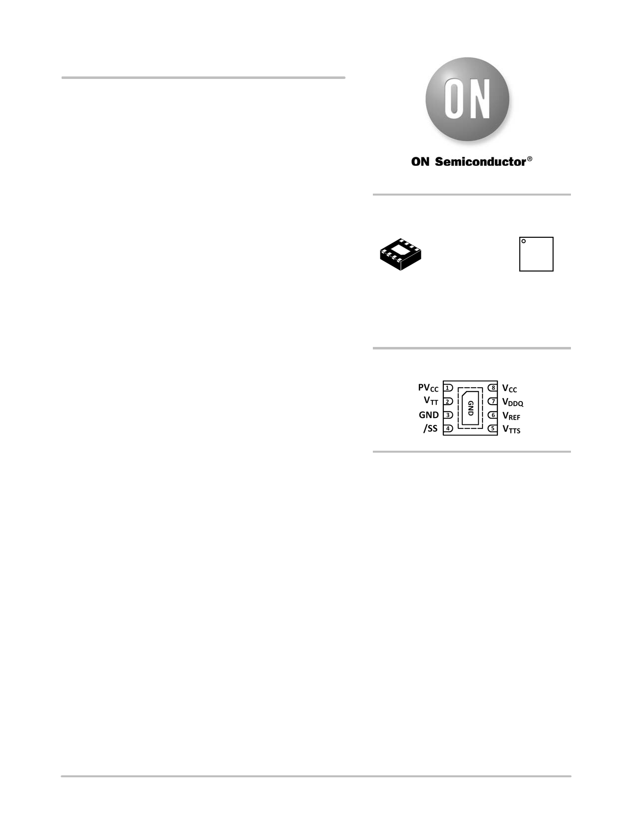
NCP51190, NCV51190
1.5A DDR Memory
Termination Regulator
The NCP/NCV51190 is a simple, cost−effective, high−speed linear
regulator designed to generate the VTT termination voltage rail for
DDR−I, DDR−II and DDR−III memory. The regulator is capable of
actively sourcing or sinking up to ±1.5 A for DDR−I, or up to ±0.5 A
for DDR−II /−III while regulating the output voltage to within
±30 mV.
The output termination voltage is tightly regulated to track VTT =
(VDDQ / 2) over the entire current range.
The NCP/NCV51190 incorporates a high−speed differential
amplifier to provide ultra−fast response to line and load transients.
Other features include extremely low initial offset voltage, excellent
load regulation, source/sink soft−start and on−chip thermal shut−down
protection.
The NCP/NCV51190 features the power−saving Suspend To Ram
(STR) function which will tri−state the regulator output and lower the
quiescent current drawn when the /SS pin is pulled low.
The NCP/NCV51190 is available in a DFN8 package.
Features
• Generate DDR Memory Termination Voltage (VTT)
• For DDR−I, DDR−II, DDR−III Source / Sink Currents
• Supports DDR−I to ±1.5 A, DDR−II, DDR−III to ±0.5 A (peak)
• Integrated Power MOSFETs with Thermal Protection
• Stable with 10 mF Ceramic VTT Capacitor
• High Accuracy Output Voltage at Full−Load
• Minimal External Component Count
• Shutdown for Standby or Suspend to RAM (STR) mode
• Built−in Soft Start
• NCV Prefix for Automotive and Other Applications Requiring
Unique Site and Control Change Requirements; AEC−Q100
Qualified and PPAP Capable
• These are Pb−Free Devices
Appications
• Desktop PC’s, Notebooks, and Workstations
• Graphics Card DDR Memory Termination
• Set Top Boxes, Digital TV’s, Printers
• Embedded Systems
• Active Bus Termination
http://onsemi.com
MARKING
DIAGRAM
DFN8
MN SUFFIX
CASE 506AA
1
XXMG
G
1
XX = Specific Device Code
M = Date Code
G = Pb−Free Device
(Note: Microdot may be in either location)
PIN CONNECTION
ORDERING INFORMATION
See detailed ordering, marking and shipping information in the
package dimensions section on page 8 of this data sheet.
© Semiconductor Components Industries, LLC, 2014
November, 2014 − Rev. 3
1
Publication Order Number:
NCP51190/D
1 page 
140
120
100
80
60
40
20
0
2
3.5
3.0
2.5
2.0
1.5
1.0
0.5
2
3.0
2.5
2.0
1.5
1.0
0.5
0
0
NCP51190, NCV51190
TYPICAL PERFORMANCE CHARACTERISTICS
3 45
VCC (V)
Figure 2. IqSD vs. VCC
3 45
VCC (V)
Figure 4. VIH and VIL
12 3 45
VDDQ (V)
Figure 6. VTT vs. VDDQ
700
600
500
400
300
200
100
0
62
345
VCC (V)
Figure 3. Iq vs. VCC
6
3.0
2.5
2.0
1.5
1.0
0.5
0
6 0123 456
VDDQ (V)
Figure 5. VREF vs. VDDQ
160
140
120
100
80
60
−40°C
40 25°C
20 85°C
125°C
0
62 3 4 5 6
VCC (V)
Figure 7. IqSD vs. VCC over Temperature
http://onsemi.com
5
5 Page | ||
| Páginas | Total 9 Páginas | |
| PDF Descargar | [ Datasheet NCV51190.PDF ] | |
Hoja de datos destacado
| Número de pieza | Descripción | Fabricantes |
| NCV51190 | 1.5A DDR Memory Termination Regulator | ON Semiconductor |
| NCV51198 | 1.5A DDR Memory Termination Regulator | ON Semiconductor |
| NCV51199 | Termination Regulator | ON Semiconductor |
| Número de pieza | Descripción | Fabricantes |
| SLA6805M | High Voltage 3 phase Motor Driver IC. |
Sanken |
| SDC1742 | 12- and 14-Bit Hybrid Synchro / Resolver-to-Digital Converters. |
Analog Devices |
|
DataSheet.es es una pagina web que funciona como un repositorio de manuales o hoja de datos de muchos de los productos más populares, |
| DataSheet.es | 2020 | Privacy Policy | Contacto | Buscar |