|
|
|
PDF THAT1571 Data sheet ( Hoja de datos )
| Número de pieza | THAT1571 | |
| Descripción | High-Performance Digital Preamplifier Controller IC | |
| Fabricantes | THAT | |
| Logotipo | ||
Hay una vista previa y un enlace de descarga de THAT1571 (archivo pdf) en la parte inferior de esta página. Total 20 Páginas | ||
|
No Preview Available !
FEATURES
y Ideal mate for THAT1570 preamplifier
y Wide gain range:
– +13.6 to +68.6dB in 1dB steps, and
– +5.6dB
y Wide supply range: ±5V to ±17V
y Wide output swing:+27dBu (±17V sup.)
y Wide input swing: +22dBu (±17V sup.)
y Low THD+N: 0.0003% @ 22dB gain
y Integrated differential servo minimizes
output offset
y Zero-crossing detector minimizes
switching noise
y Flexible, addressable SPI interface
y Four general-purpose digital outputs
y Small 7mm x 7mm QFN32 package
High-Performance Digital
Preamplifier Controller IC
THAT 5171
APPLICATIONS
y Digitally controlled microphone
preamplifiers
y Digitally-controlled instrumentation
amplifiers
y Digitally-controlled differential
amplifiers
y Audio mixing consoles
y PC audio breakout boxes
y Audio distribution systems
y Digital audio snakes
y Portable audio recorders
Description
The THAT5171 is a digital gain controller for
low-noise, analog, differential, current-feedback
audio preamplifiers such as the THAT 1570.
When used in conjunction with an appropriate
analog gain block, the 5171 can set gain to
5.6dB, or any gain from 13.6dB to 68.6dB in 1dB
steps, while preserving low noise and distortion.
It operates from ±5V to ±17V supplies, support-
ing input signal levels as high as +22 dBu (at
5.6dB gain, and ±17V supplies) in combination
with the 1570 (without an external input pad).
The 5171 includes a differential servo and zero-
crossing detector to minimize dc offsets and
glitches (zipper noise) during gain adjustments.
The 5171 is controlled via an addressable
serial-peripheral interface (SPI) port. Four Gen-
eral Purpose Outputs (GPOs) can be controlled
via this interface. The GPOs may be connected to
input pads, analog switches, mute circuits, LEDs,
etc. The SPI bus supports read-back so that host
software can verify proper operation.
The 5171 was designed to mate perfectly with
the THAT 1570 Differential Audio Preamplifier
IC. Together, these two ICs provide a best-of-
class solution for digitally-controllable audio pre-
amplifier applications. However, for designers
who prefer a more customized solution, the 5171
may also be used to control a discrete preampli-
fier.
Fabricated in a high-voltage CMOS process,
the 5171 integrates an astonishing amount of cir-
cuitry within a very small package. It comes in a
small (7x7 mm) 32-pin QFN package, making it
suitable for small portable devices.
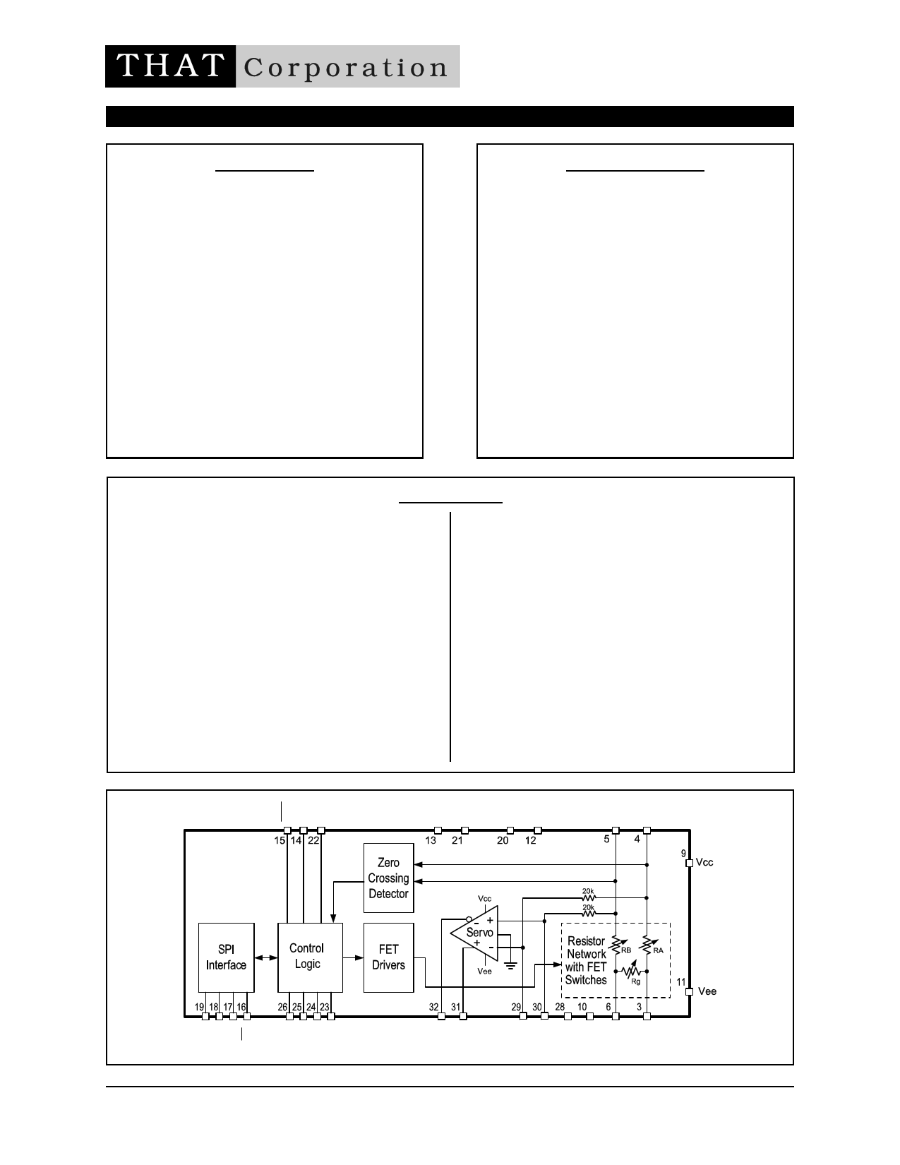
Figure 1. THAT 5171 Block Diagram
THAT Corporation; 45 Sumner Street; Milford, MA 01757-1656; USA
Tel: +1 508 478 9200; Fax: +1 508 478 0990; Web: www.thatcorp.com
Copyright © 2014, THAT Corporation Document 600133 Rev 08
1 page 
THAT5171 High-Performance
Digital Preamplifier Controller IC
Page 5 of 20
Document 600133 Rev 08
Theory of Operation
The THAT 5171 is a gain controller in the form of
a digitally controlled differential attenuator; it is not
an amplifier. It contains a set of precision resistors,
switched by a set of CMOS FET switches, configured
to create a variable, switched, differential attenuation
network. The network’s impedances are ideal for
controlling gain in low-voltage-noise, current-feed-
back instrumentation amplifiers, and are optimized
for low source impedance applications. For example,
when coupled with a low-noise gain stage like the
THAT 1570, it maintains 1.5nV/√Hz noise floor at
68.6dB gain in the complete circuit.
Using the 5171
The attenuator is intended primarily for use in
the feedback loop of differential current-feedback
gain stages, such as the THAT 1570. Designed spe-
cifically for use in high-performance microphone pre-
amplifiers, THAT’s engineers paid careful attention
to precision, stability, and control over the resistors
and their switches, in order to maintain excellent
audio performance over a wide range of gains and
signal levels.
U1
THAT5171
U2
THAT1570
Figure 2. Analog portion of 5171 connected to a 1570.
Figure 2 shows the analog portion of the 5171
connected to a 1570. Resistors RA, RB, and RG form a
differential attenuator (“U-pad”). The 1570’s differen-
tial output is applied to RA and RB. The output of the
attenuator, appearing across RG, is connected to the
inverting differential input of the dual current-
feedback amplifiers in the 1570 (the RG1 and RG2
pins). The voltage divider ratio thus controls the dif-
ferential gain of the circuit.
The 5171 changes the attenuator settings based
on the gain command provided via the SPI control
interface. At minimum gain, RG is ~7.93kΩ, while
RA = RB = ~3.56kΩ, which sets the circuit gain to
+5.6dB. To achieve other gains, all three resistors
are varied by CMOS switches in order to produce
1dB gain steps from +13.6 to +68.5dB. At all gains,
the impedance levels are chosen to minimize noise
and distortion within the circuit as a whole.
Table 2 lists the typical internal attenuator resis-
tor values for each gain setting.
Gain
Setting
5.6
13.6
14.6
15.6
16.6
17.6
18.6
19.6
20.6
21.6
22.6
23.6
24.6
25.6
26.6
27.6
28.6
29.6
30.6
31.6
32.6
33.6
34.6
35.6
36.6
37.6
38.6
39.6
40.6
41.6
42.6
43.6
44.6
45.6
46.6
47.6
48.6
49.6
50.6
51.6
52.6
53.6
54.6
55.6
56.6
57.6
58.6
59.6
60.6
61.6
62.6
63.6
64.6
65.6
66.6
67.6
68.6
Rg
(ohms)
7.9k
1.4k
1.4k
1.4k
1.4k
1.4k
1.4k
1.4k
1.4k
560
560
560
560
560
560
560
560
220
220
220
220
220
220
220
220
89
89
89
89
89
89
89
89
35
35
35
35
35
35
35
35
14
14
14
14
14
14
14
14
5.6
5.6
5.6
5.6
5.6
5.6
5.6
5.6
Ra, Rb
(ohms)
3.6k
2.7k
3.1k
3.5k
4.0k
4.6k
5.3k
6.0k
6.8k
3.1k
3.5k
3.9k
4.5k
5.0k
5.7k
6.4k
7.2k
3.2k
3.7k
4.1k
4.6k
5.2k
5.9k
6.6k
7.4k
3.3k
3.7k
4.2k
4.7k
5.3k
5.9k
6.7k
7.5k
3.3k
3.8k
4.2k
4.7k
5.3k
6.0k
6.7k
7.5k
3.4k
3.8k
4.2k
4.7k
5.3k
6.0k
6.7k
7.5k
3.4k
3.8k
4.2k
4.7k
5.3k
6.0k
6.7k
7.5k
“Gain”
Register
0
8
9
10
11
12
13
14
15
16
17
18
19
20
21
22
23
24
25
26
27
28
29
30
31
32
33
34
35
36
37
38
39
40
41
42
43
44
45
46
47
48
49
50
51
52
53
54
55
56
57
58
59
60
61
62
63
Table 2. Internal attenuator resistor values.
THAT Corporation; 45 Sumner Street; Milford, MA 01757-1656; USA
Tel: +1 508 478 9200; Fax: +1 508 478 0990; Web: www.thatcorp.com
Copyright © 2014, THAT Corporation; All rights reserved.
5 Page 
THAT5171 High-Performance
Digital Preamplifier Controller IC
Page 11 of 20
Document 600133 Rev 08
THAT recommends one decoupling capacitor
(C16) for the digital power supply, placed close to
pins 20 (DGND) and 21 (VDD), as these pins connect to
the digital output driver bus. Pins 12 (DGND) and Pin
13 (VDD) should be connected to pins 20 and 21,
respectively, through short, low-inductance paths.
AGND and DGND should be connected together
directly under the 5171. Note that the part includes
back-to-back diodes limiting the maximum voltage
difference between these nodes. If even on a transient
basis (e.g., supply spikes) a voltage difference of over
0.5 V exists between AGND and DGND, large currents
will flow which may damage the part.
As described above (in the Theory section), the
integrated differential servo is required for proper
operation of the system as shown in the application
schematics. By using the servo amplifier in feedback,
output offset can be controlled over a wide range of
gains.
In order to optimize settling behavior, THAT rec-
ommends that C12 and C13 be approximately one-half
the size of C4 and C5. As well, to avoid the servo from
contributing noise to the preamplifier, we recom-
mend that the servo’s output be divided down by
approximately 1000:1 by the combination of R7/R1
and R8/R2.
Zero Crossing Detector
The integrated zero-crossing detector may be
enabled or disabled. (See the digital control section
below for details.) When enabled, it prevents gain
changes from occurring until the differential output
signal waveform is within ±5mV of zero. It is possible
that in unusual cases where significant low-frequency
material is present, the zero-crossing detector may
unacceptably delay a gain change from taking place.
A timeout, set by RT and CT, is provided to force a
gain change to occur within RTCTmS of the time it is
requested, even if zero crossing is enabled.
Digital Control
Reset (RST pin)
Asserting the RST pin low forces all internal reg-
isters to their default state (see register definitions in
SPI Port section for default values after reset). This
pin is typically connected to system reset or to a port
on the host microcontroller.
During reset, the 5171 reads the 3-bit SPI
address via the GPO[2:0] pins. These pins are typi-
cally connected to pull-up and pull-down resistors to
establish the chip address, and serve as general pur-
pose outputs during runtime. THAT Corporation
intends to offer features in future versions of the
5171 that will be configured via a pull up resistor on
GPO3. Thus, GPO3 should be pulled low by a resis-
tor of 100 kΩ or less on early designs before these
new features become available.
Busy (BSY pin)
The BSY pin is asserted high when the current
gain setting is not equal to the value in the GAIN reg-
ister, i.e. when a gain update is pending a zero-
crossing. This pin may be monitored by the host
microcontroller (e.g. connected to an external inter-
rupt pin) in order to hold off a new gain command
until the previous gain command has been executed.
Note that in ZERO-CROSSING mode, the BSY pin
goes low when a pending gain change has been made.
If finer gain steps are implemented in subsequent
processing (typically via DSP) this signal can be used
to assist in synchronizing subsequent gain changes
with those implemented by the 5171. Note, of course,
that latency in A/D conversion must be considered
when attempting to synchronize digital with analog
gain updates.
Gain Update Modes (and TRC pin)
The 5171 supports two gain update modes,
selected by the MODE bits in the Control/Status Reg-
ister (Table 13), as follows.
1) IMMEDIATE Mode: Gain updates are made
immediately following a rising edge on the /CS
pin.
2) ZERO-CROSSING Mode: Updates are made on
the next output signal zero-crossing after a rising
edge on the /CS pin. An RC time constant con-
nected to the TRC pin (RT/CT in Figures 3~6)
establishes a time-out period in case a zero-
crossing does not occur within a desired time
window. The zero-crossing time-out function
operates as follows:
Signal
CS
SCLK
DIN
DOUT
Pin I/O
16 Input
Function
Device chip select input, active low. An SPI transfer begins with a high-to-low
CS transition and ends with a low-to-high CS transition. When CS is high,
SCLK transitions are ignored. Zero-crossing timeout capacitor CT is dis-
charged when CS goes low.
17 Input
SPI serial clock input. An SPI master supplies this clock with frequencies up
to 10MHz. Data is clocked into the DIN pin on the rising edge of SCLK. Data
is clocked out of DOUT pin on the falling edge of SCLK.
18 Input
SPI serial data input (Master-Out, Slave-In). DIN is MSB first.
19
Output/Tristate
SPI serial data output (Master-In, Slave-Out). DOUT is a tristate output.
DOUT is tristated when CS is high. DOUT is MSB first.
Table 3. SPI signals.
THAT Corporation; 45 Sumner Street; Milford, MA 01757-1656; USA
Tel: +1 508 478 9200; Fax: +1 508 478 0990; Web: www.thatcorp.com
Copyright © 2014, THAT Corporation; All rights reserved.
11 Page | ||
| Páginas | Total 20 Páginas | |
| PDF Descargar | [ Datasheet THAT1571.PDF ] | |
Hoja de datos destacado
| Número de pieza | Descripción | Fabricantes |
| THAT1570 | Audio Preamplifier IC | THAT |
| THAT1571 | High-Performance Digital Preamplifier Controller IC | THAT |
| Número de pieza | Descripción | Fabricantes |
| SLA6805M | High Voltage 3 phase Motor Driver IC. |
Sanken |
| SDC1742 | 12- and 14-Bit Hybrid Synchro / Resolver-to-Digital Converters. |
Analog Devices |
|
DataSheet.es es una pagina web que funciona como un repositorio de manuales o hoja de datos de muchos de los productos más populares, |
| DataSheet.es | 2020 | Privacy Policy | Contacto | Buscar |