|
|
|
PDF NCP330 Data sheet ( Hoja de datos )
| Número de pieza | NCP330 | |
| Descripción | Soft-Start Controlled Load Switch | |
| Fabricantes | ON Semiconductor | |
| Logotipo | ||
Hay una vista previa y un enlace de descarga de NCP330 (archivo pdf) en la parte inferior de esta página. Total 9 Páginas | ||
|
No Preview Available !
NCP330
Soft-Start Controlled Load
Switch
The NCP330 is a low Ron N−channel MOSFET controlled by a
soft−start sequence of 2 ms for mobile applications.
The very low RDS(on) allows system supplying or battery charging
up to DC 3A.The device is enable automatically if a Power Supply is
connected on Vin pin (active High) and maintained off if no Vin
(internal pull down).
Due to a current consumption optimization, leakage current is
drastically decreased from the battery connected to the device,
allowing long battery life.
Features
• 1.8 V − 5.5 V Operating Range
• 30 mW N−MOSFET
• DC Current Up to 3 A
• Peak Current Up to 5 A
• Built−in Soft−Start 2 ms
• Reverse Voltage Protection
• Active High with Integrated Bridge
• Compliance to IEC61000−4−2 (Level 4)
8.0 kV (Contact)
15 kV (Air)
• ESD Ratings: Machine Model = B
Human Body Model = 3
• mDFN4 1.2 x 1.6 mm
• NCV Prefix for Automotive and Other Applications Requiring
Unique Site and Control Change Requirements; AEC−Q100
Qualified and PPAP Capable
• This is a Pb−Free Device
Typical Applications
• Mobile Phones
• Tablets
• Digital Cameras
• GPS
• Computers
Vbat
1 mF
IN OUT
NCP330
1 mF
EN GND
EN
www.onsemi.com
1
UDFN4
CASE 517CE
MARKING
DIAGRAM
3A M
3A = Specific Device Code
M = Date Code
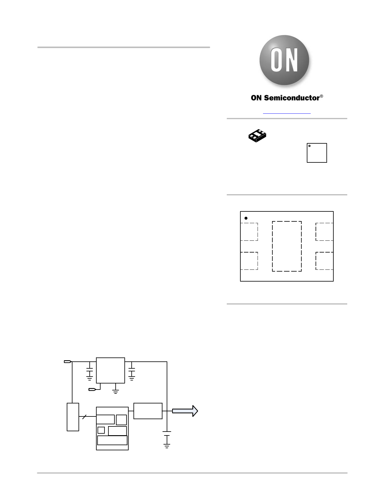
PINOUT DIAGRAM
IN
GND
PAD1
OUT
EN
(Top View)
ORDERING INFORMATION
See detailed ordering and shipping information on page 8 of
this data sheet.
VBUS
USB D+
Port D−
GND
4
IN CMIC OUT
Supply HS
Monitoring USB
I@C Signal
Routing
Accessory
Detection and ID
SBC Charger
SYSTEM
Figure 1. Typical Application Circuit
© Semiconductor Components Industries, LLC, 2015
April, 2015 − Rev. 2
1
Publication Order Number:
NCP330/D
1 page 
NCP330
TYPICAL CHARACTERISTICS
140
TA = 85°C
120
TA = 25°C
100
80 TA = −40°C
60
40
20
0
1.5 2.0 2.5 3.0 3.5 4.0 4.5 5.0
VIN, INPUT VOLTAGE (V)
Figure 3. Supply Current vs. Voltage
5.5
0.35
0.30
0.25
0.20
TA = 85°C
0.15
0.10
TA = −40°C
0.05
0 TA = 25°C
1.5 2.0 2.5 3.0 3.5 4.0 4.5 5.0 5.5
VOUT, OUTPUT VOLTAGE (V)
Figure 4. Reverse Current vs. Output Voltage
50
45
40
35 IOUT = 3 A
IOUT = 2 A
30 IOUT = 1 A
IOUT = 0.5 A
25
20
1.8 3.0 4.2 5.4
VIN, INPUT VOLTAGE (V)
Figure 5. RDS(on) vs. VIN Voltage at 255C
50
45
40
35
30
25
20
1.8
IOUT = 2 A
IOUT = 3 A
IOUT = 1 A IOUT = 0.5 A
3.0 4.2 5.4
VIN, INPUT VOLTAGE (V)
Figure 7. RDS(on) vs. VIN Voltage at −405C
50
45 IOUT = 2 A
IOUT = 3 A
40
IOUT = 0.5 A
35 IOUT = 1 A
30
25
20
1.8 3.0 4.2 5.4
VIN, INPUT VOLTAGE (V)
Figure 6. RDS(on) vs. VIN Voltage at 855C
50
45
40 VIN = 1.8 V
35
VIN = 3.0 V
30 VIN = 5.5 V
25 VIN = 5.0 V
20
0 0.5 1.0 1.5 2.0 2.5 3.0
IOUT, OUTPUT CURRENT (A)
Figure 8. RDS(on) vs. IOUT at 255C
3.5
www.onsemi.com
5
5 Page | ||
| Páginas | Total 9 Páginas | |
| PDF Descargar | [ Datasheet NCP330.PDF ] | |
Hoja de datos destacado
| Número de pieza | Descripción | Fabricantes |
| NCP330 | Soft-Start Controlled Load Switch | ON Semiconductor |
| NCP333 | 1.5A Ultra-Small Controlled Load Switch | ON Semiconductor |
| NCP3334 | Adjustable Low Dropout Regulator | ON Semiconductor |
| NCP3334A | Low Dropout Regulator | ON Semiconductor |
| Número de pieza | Descripción | Fabricantes |
| SLA6805M | High Voltage 3 phase Motor Driver IC. |
Sanken |
| SDC1742 | 12- and 14-Bit Hybrid Synchro / Resolver-to-Digital Converters. |
Analog Devices |
|
DataSheet.es es una pagina web que funciona como un repositorio de manuales o hoja de datos de muchos de los productos más populares, |
| DataSheet.es | 2020 | Privacy Policy | Contacto | Buscar |