|
|
|
PDF BL93C46 Data sheet ( Hoja de datos )
| Número de pieza | BL93C46 | |
| Descripción | Two-wire Serial EEPROM | |
| Fabricantes | BELLING | |
| Logotipo | ||
Hay una vista previa y un enlace de descarga de BL93C46 (archivo pdf) en la parte inferior de esta página. Total 12 Páginas | ||
|
No Preview Available !
Shanghai Belling Corp., Ltd
BL93C46
1K bits (128 X 8 or 64 X 16) Three-wire Serial EEPROM
Features
Three-wire Serial Interface
VCC = 1.8V to 5.5V
2 MHz Rate (5V) Compatibility
Self-timed Write Cycle (5 ms max)
1 Million Write Cycles guaranteed
Data Retention > 100 Years
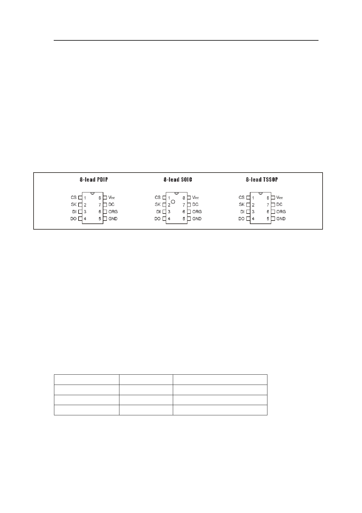
8-lead PDIP, 8-lead JEDEC SOIC and 8-lead TSSOP Packages
BL93C46
Description
The BL93C46 provides 1024 bits of serial electrically erasable programmable read only memory (EEPROM)
organized as 64 words of 16 bits each, when the ORG pin is connected to VCC and 128 words of 8 bits each
when it is tied to ground. TheBL93C46 is available in space-saving 8-lead PDIP, 8-lead TSSOP and 8-lead
JEDEC SOIC packages. The BL93C46 is enabled through the Chip Select pin (CS), and accessed via a 3-wire
serial interface consisting of Data Input (DI), Data Output (DO), and Shift Clock (SK). Upon receiving a Read
instruction at DI, the address is decoded and the data is clocked out serially on the data output pin DO. The
WRITE cycle is completely self-timed and no separate erase cycle is required before write. The Write cycle is
only enabled when it is in the Erase/Write Enable state. When CS is brought “high” following the initiation of a
write cycle, the DO pin outputs the Ready/Busy status.
Order information
Part Number
BL93C46-DIP
BL93C46-SOP
BL93C46-TSSOP
Package
PDIP8
SOP8
TSSOP8
shipping
tube
tube 2500 pcs / Tape & Reel
tube 3000 pcs / Tape & Reel
1
1 page 
Shanghai Belling Corp., Ltd
BL93C46
Functional Description
The BL93C46 is accessed via a simple and versatile three-wire serial communication interface. Device
operation is controlled by seven instructions issued by the host processor. A valid instruction starts with a
rising edge of CS and consists of a start bit (logic“1”) followed by the appropriate op code and the desired
memory address location.
READ (READ): The Read (READ) instruction contains the address code for the memory location to be read.
After the instruction and address are decoded, data from the selected memory location is available at the
serial output pin DO. Output data changes are synchronized with the rising edges of serial clock SK. It should
be noted that a dummy bit (logic “0”) precedes the 8- or 16-bit data output string.
ERASE/WRITE (EWEN): To assure data integrity, the part automatically goes into the Erase/Write Disable
(EWDS) state when power is first applied. An Erase/Write Enable(EWEN) instruction must be executed first
before any programming instructions can be carried out. Please note that once in the EWEN state,
programming remains enabled until an EWDS instruction is executed or VCC power is removed from the part.
ERASE (ERASE): The Erase (ERASE) instruction programs all bits in the specified memory location to the
logical “1” state. The self-timed erase cycle starts once the ERASE instruction and address are decoded. The
DO pin outputs the Ready/Busy status of the part if CS is brought high after being kept low for a minimum of
250 ns (TCS). A logic “1” at pin DO indicates that the selected memory location has been erased, and the part
is ready for another instruction.
WRITE (WRITE): The Write (WRITE) instruction contains the 8 or 16 bits of data to be written into the
specified memory location. The self-timed programming cycle, tWP, starts after the last bit of data is received
at serial data input pin DI. The DO pin outputs the Ready/Busy status of the part if CS is brought high after
being kept low for a minimum of 250 ns (TCS). A logic “0” at DO indicates that programming is still in progress.
A logic “1” indicates that the memory location at the specified address has been written with the data pattern
contained in the instruction and the part is ready for further instructions. A Ready/Busy status cannot be
obtained if the CS is brought high after the end of the selftimed programming cycle, TWP.
ERASE ALL (ERAL): The Erase All (ERAL) instruction programs every bit in the memory array to the logic “1”
state and is primarily used for testing purposes. The DO pin outputs the Ready/Busy status of the part if CS is
5
5 Page 
Shanghai Belling Corp., Ltd
8-lead TSSOP Outline Dimensions
BL93C46
SYMBOL
A
A1
A2
A3
b
b1
c
c1
D
E
MILLIMETER
MIN NOM MAX
- - 1.20
0.05 - 0.15
0.90 1.00 1.05
0.34 0.44 0.54
0.20 - 0.28
0.20 0.22 0.24
0.10 - 0.19
0.10 0.13 0.15
2.83 2.93 3.03
6.20 6.40 6.60
11
11 Page | ||
| Páginas | Total 12 Páginas | |
| PDF Descargar | [ Datasheet BL93C46.PDF ] | |
Hoja de datos destacado
| Número de pieza | Descripción | Fabricantes |
| BL93C46 | Two-wire Serial EEPROM | BELLING |
| Número de pieza | Descripción | Fabricantes |
| SLA6805M | High Voltage 3 phase Motor Driver IC. |
Sanken |
| SDC1742 | 12- and 14-Bit Hybrid Synchro / Resolver-to-Digital Converters. |
Analog Devices |
|
DataSheet.es es una pagina web que funciona como un repositorio de manuales o hoja de datos de muchos de los productos más populares, |
| DataSheet.es | 2020 | Privacy Policy | Contacto | Buscar |