|
|
|
PDF KS8995X Data sheet ( Hoja de datos )
| Número de pieza | KS8995X | |
| Descripción | Integrated 5-Port 10/100 QoS Switch | |
| Fabricantes | Micrel Semiconductor | |
| Logotipo | ||
Hay una vista previa y un enlace de descarga de KS8995X (archivo pdf) en la parte inferior de esta página. Total 30 Páginas | ||
|
No Preview Available !
KS8995X
Micrel
KS8995X
Integrated 5-Port 10/100 QoS Switch
Rev. 1.13
General Description
The KS8995X is a highly integrated Layer-2 QoS (Quality of
Service) switch with optimized BOM (Bill of Materials) cost for
low port count, cost-sensitive 10/100Mbps switch systems. It
also provides an extensive feature set including three differ-
ent QoS priority schemes, a dual MII interface for BOM cost
reduction, rate limiting to offload CPU tasks, software and
hardware power-down, a MDC/MDIO control interface and
port mirroring/monitoring to effectively address both current
and emerging Fast Ethernet applications.
The KS8995X contains five 10/100 transceivers with pat-
ented mixed-signal low-power technology, five MAC (Media
Access Control) units, a high-speed non-blocking switch
fabric, a dedicated address lookup engine, and an on-chip
frame buffer memory.
All PHY units support 10BaseT and 100BaseTX. In addition,
two of the PHY units support 100BaseFX (Ports 4 and 5).
All support documentation can be found on Micrel’s web site
at www.micrel.com.
Features
• Integrated switch with five MACs and five Fast Ethernet
transceivers fully compliant to IEEE 802.3u standard
• Shared memory based switch fabric with fully non-
blocking configuration
• 10BaseT, 100BaseTX and 100BaseFX modes (FX in
Ports 4 and 5)
• Dual MII configuration: MII-Switch (MAC or PHY mode
MII) and MII-P5 (PHY mode MII)
• VLAN ID tag/untag options, per-port basis
• Enable/disable option for huge frame size up to 1916
bytes per frame
• Broadcast storm protection with percent control – global
and per-port basis
• Optimization for fiber-to-copper media conversion
• Full-chip hardware power-down support (register
configuration not saved)
• Per-port-based software power-save on PHY (idle link
detection, register configuration preserved)
• QoS/CoS packets prioritization supports: per port,
802.1p and DiffServ based
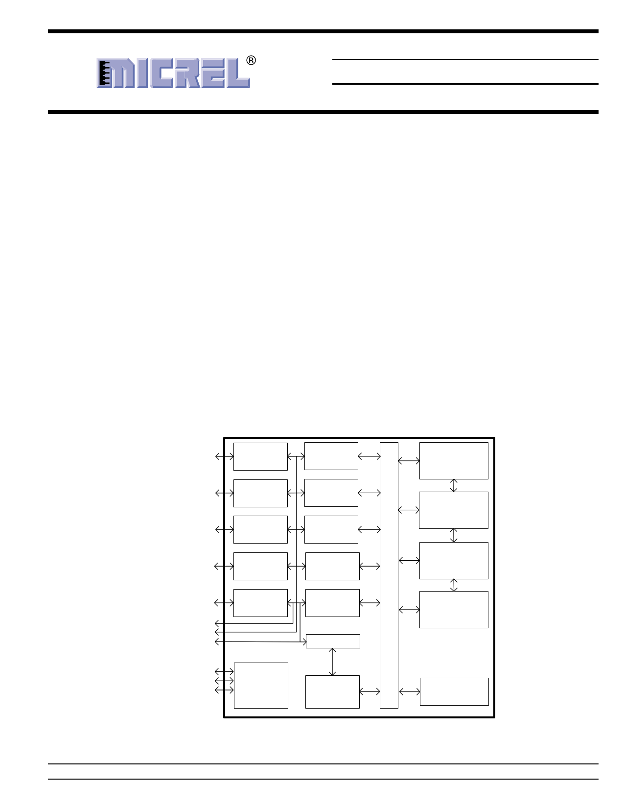
Functional Diagram
Auto
MDI/MDIX
Auto
MDI/MDIX
Auto
MDI/MDIX
Auto
MDI/MDIX
Auto
MDI/MDIX
MII-P5
MDC, MDI/O
MII-SW or SNI
LED0[5:1]
LED1[5:1]
LED2[5:1]
10/100
T/Tx 1
10/100
T/Tx 2
10/100
T/Tx 3
10/100
T/Tx/Fx 4
10/100
T/Tx/Fx 5
LED I/F
10/100
MAC 1
10/100
MAC 2
10/100
MAC 3
10/100
MAC 4
10/100
MAC 5
SNI
Control
Registers
1K look-up
Engine
Queue
Mgmnt
Buffer
Mgmnt
Frame
Buffers
EEPROM
I/F
Micrel, Inc. • 1849 Fortune Drive • San Jose, CA 95131 • USA • tel + 1 (408) 944-0800 • fax + 1 (408) 944-0970 • http://www.micrel.com
December 2003
1
M9999-120403
1 page 
KS8995X
Micrel
Register 8 (0x08): Global Control 6 ................................................................................................................................ 32
Register 9 (0x09): Global Control 7 ................................................................................................................................ 32
Register 10 (0x0A): Global Control 8 ............................................................................................................................. 32
Register 11 (0x0B): Global Control 9 ............................................................................................................................. 33
Port Registers .......................................................................................................................................................................... 33
Register 16 (0x10): Port 1 Control 0 .............................................................................................................................. 33
Register 17 (0x11): Port 1 Control 1 .............................................................................................................................. 34
Register 18 (0x12): Port 1 Control 2 .............................................................................................................................. 34
Register 19 (0x13): Port 1 Control 3 .............................................................................................................................. 35
Register 20 (0x14): Port 1 Control 4 .............................................................................................................................. 35
Register 21 (0x15): Port 1 Control 5 .............................................................................................................................. 35
Register 22 (0x16): Port 1 Control 6 .............................................................................................................................. 35
Register 23 (0x17): Port 1 Control 7 .............................................................................................................................. 36
Register 24 (0x18): Port 1 Control 8 .............................................................................................................................. 36
Register 25 (0x19): Port 1 Control 9 .............................................................................................................................. 36
Register 26 (0x1A): Port 1 Control 10 ............................................................................................................................ 36
Register 27 (0x1B): Port 1 Control 11 ............................................................................................................................ 37
Register 28 (0x1C): Port 1 Control 12 ............................................................................................................................ 37
Register 29 (0x1D): Port 1 Control 13 ............................................................................................................................ 38
Register 30 (0x1E): Port 1 Status 0 ............................................................................................................................... 39
Register 31 (0x1F): Port 1 Status 1 ................................................................................................................................ 39
Advanced Control Registers .................................................................................................................................................... 39
Register 96 (0x60): TOS Priority Control Register 0 ...................................................................................................... 39
Register 97 (0x61): TOS Priority Control Register 1 ...................................................................................................... 39
Register 98 (0x62): TOS Priority Control Register 2 ...................................................................................................... 39
Register 99 (0x63): TOS Priority Control Register 3 ...................................................................................................... 39
Register 100 (0x64): TOS Priority Control Register 4 .................................................................................................... 39
Register 101 (0x65): TOS Priority Control Register 5 .................................................................................................... 39
Register 102 (0x66): TOS Priority Control Register 6 .................................................................................................... 40
Register 103 (0x67): TOS Priority Control Register 7 .................................................................................................... 40
Register 104 (0x68): MAC Address Register 0 .............................................................................................................. 40
Register 105 (0x69): MAC Address Register 1 .............................................................................................................. 40
Register 106 (0x6A): MAC Address Register 2 .............................................................................................................. 40
Register 107 (0x6B): MAC Address Register 3 .............................................................................................................. 40
Register 108 (0x6C): MAC Address Register 4 ............................................................................................................. 40
Register 109 (0X6D): MAC Address Register 5 ............................................................................................................. 40
MIIM Registers ........................................................................................................................................................................ 40
Register 0: MII Control ................................................................................................................................................... 40
Register 1: MII Status .................................................................................................................................................... 41
Register 2: PHYID HIGH ................................................................................................................................................ 41
Register 3: PHYID LOW ................................................................................................................................................ 41
Register 4: Advertisement Ability ................................................................................................................................... 41
Register 5: Link Partner Ability ....................................................................................................................................... 42
Absolute Maximum Ratings .......................................................................................................................................................... 43
Operating Ratings .......................................................................................................................................................................... 43
Electrical Characteristics .............................................................................................................................................................. 43
Timing Diagrams ............................................................................................................................................................................ 45
Selection of Isolation Transformers ............................................................................................................................................. 50
Package Information ...................................................................................................................................................................... 51
December 2003
5
M9999-120403
5 Page 
KS8995X
Micrel
Pin Number
86
Pin Name
SCONF1
87 SCONF0
88 GNDD
89 VDDC
90 LED5-2
91 LED5-1
92 LED5-0
93 LED4-2
94 LED4-1
95 LED4-0
96 LED3-2
97 LED3-1
98 LED3-0
99 GNDD
100 VDDIO
101 LED2-2
102 LED2-1
103 LED2-0
104 LED1-2
105 LED1-1
106 LED1-0
107 MDC
108 MDIO
Type(1)
Ipd
Ipd
Gnd
P
Ipu/O
Ipu/O
Ipu/O
Ipu/O
Ipu/O
Ipu/O
Ipu/O
Ipu/O
Ipu/O
Gnd
P
Ipu/O
Ipu/O
Ipu/O
Ipu/O
Ipu/O
Ipu/O
Ipu
Ipu/O
Port
5
5
5
4
4
4
3
3
3
2
2
2
1
1
1
All
All
Pin Function
Dual MII configuration pin.
Pin# (91, 86, 87):
Switch MII
PHY [5] MII
000
Disable, Otri
Disable, Otri
001
PHY Mode MII
Disable, Otri
010
MAC Mode MII
Disable, Otri
011
PHY Mode SNI
Disable, Otri
100
Disable
Disable
101
PHY Mode MII
PHY Mode MII
110
MAC Mode MII
PHY Mode MII
111
PHY Mode SNI
PHY Mode MII
Dual MII configuration pin.
Digital ground
1.8V digital core VDD
LED indicator 2. Aging setup. See “Aging” section.
LED indicator 1. Strap option: PU (default): enable PHY MII I/F
PD: tristate all PHY MII output. See “pin# 86 SCONF1.”
LED indicator 0
LED indicator 2
LED indicator 1
LED indicator 0
LED indicator 2
LED indicator 1
LED indicator 0
Digital ground
3.3/2.5V digital VDD for digital I/O.
LED indicator 2
LED indicator 1
LED indicator 0
LED indicator 2
LED indicator 1
LED indicator 0
Switch or PHY[5] MII management data clock.
Switch or PHY[5] MII management data I/O.
Note:
1. P = Power supply
I = Input
O = Output
I/O = Bi-directional
Gnd = Ground
Ipu = Input w/internal pull-up
Ipd = Input w/internal pull-down
Ipd/O = Input w/internal pull-down during reset, output pin otherwise
Ipu/O = Input w/internal pull-up during reset, output pin otherwise
PU = Strap pin pull-up
PD = Strap pull-down
Otri = Output tristated
December 2003
11
M9999-120403
11 Page | ||
| Páginas | Total 30 Páginas | |
| PDF Descargar | [ Datasheet KS8995X.PDF ] | |
Hoja de datos destacado
| Número de pieza | Descripción | Fabricantes |
| KS8995 | 5 Port 10/100 Switch with PHY | ETC |
| KS8995FQ | Integrated 5-Port 10/100 Managed Switch | Micrel Semiconductor |
| KS8995FQ | Integrated 5-Port 10/100 Managed Switch | Micrel Semiconductor |
| KS8995M | 5 Port 10/100 Switch with PHY | ETC |
| Número de pieza | Descripción | Fabricantes |
| SLA6805M | High Voltage 3 phase Motor Driver IC. |
Sanken |
| SDC1742 | 12- and 14-Bit Hybrid Synchro / Resolver-to-Digital Converters. |
Analog Devices |
|
DataSheet.es es una pagina web que funciona como un repositorio de manuales o hoja de datos de muchos de los productos más populares, |
| DataSheet.es | 2020 | Privacy Policy | Contacto | Buscar |