|
|
|
PDF FL663MX Data sheet ( Hoja de datos )
| Número de pieza | FL663MX | |
| Descripción | Primary-Side-Regulation PWM Controller | |
| Fabricantes | Fairchild Semiconductor | |
| Logotipo | ||
Hay una vista previa y un enlace de descarga de FL663MX (archivo pdf) en la parte inferior de esta página. Total 14 Páginas | ||
|
No Preview Available !
June 2015
FL663
Primary-Side-Regulation PWM Controller for
LED Illumination
Features
Low Standby Power: < 30 mW
High-Voltage Startup
Few External Component Counts
Constant-Voltage (CV) and Constant-Current (CC)
Control without Secondary-Feedback Circuitry
Green-Mode: Linearly-Decreasing PWM Frequency
with Cycle skipping.
Fixed PWM Frequency at 50 kHz and 33 kHz with
Proprietary Frequency Hopping to Solve EMI
Problems
Peak-Current-Mode Control in CV Mode
Cycle-by-Cycle Current Limiting
VDD Over-Voltage Protection (OVP)
VDD Under-Voltage Lockout (UVLO)
Adjustable Brownout Detector
Gate Output Maximum Voltage Clamped at 15 V
Thermal Shutdown (TSD) Protection
Available in the 8-Lead SOIC Package
Applications
LED Illumination
Battery chargers for cellular phones, cordless
phones, PDA, digital cameras, power tools
Description
This third-generation Primary-Side-Regulation (PSR)
and highly integrated PWM controller provides features
to enhance the performance of LED illumination.
The proprietary topology, TRUECURRENT®, enables
precise CC regulation and simplified circuit for LED
illumination applications. The result is lower-cost and
smaller LED lighting compared to a conventional design
or a linear transformer.
To minimize standby power consumption, the
proprietary green-mode function provides off-time
modulation to linearly decrease PWM frequency with
cycle skipping under light-load conditions. Green mode
assists the power supply in meeting the power
conservation requirements.
By using the FL663, LED illumination can be
implemented with few external components and
minimized cost.
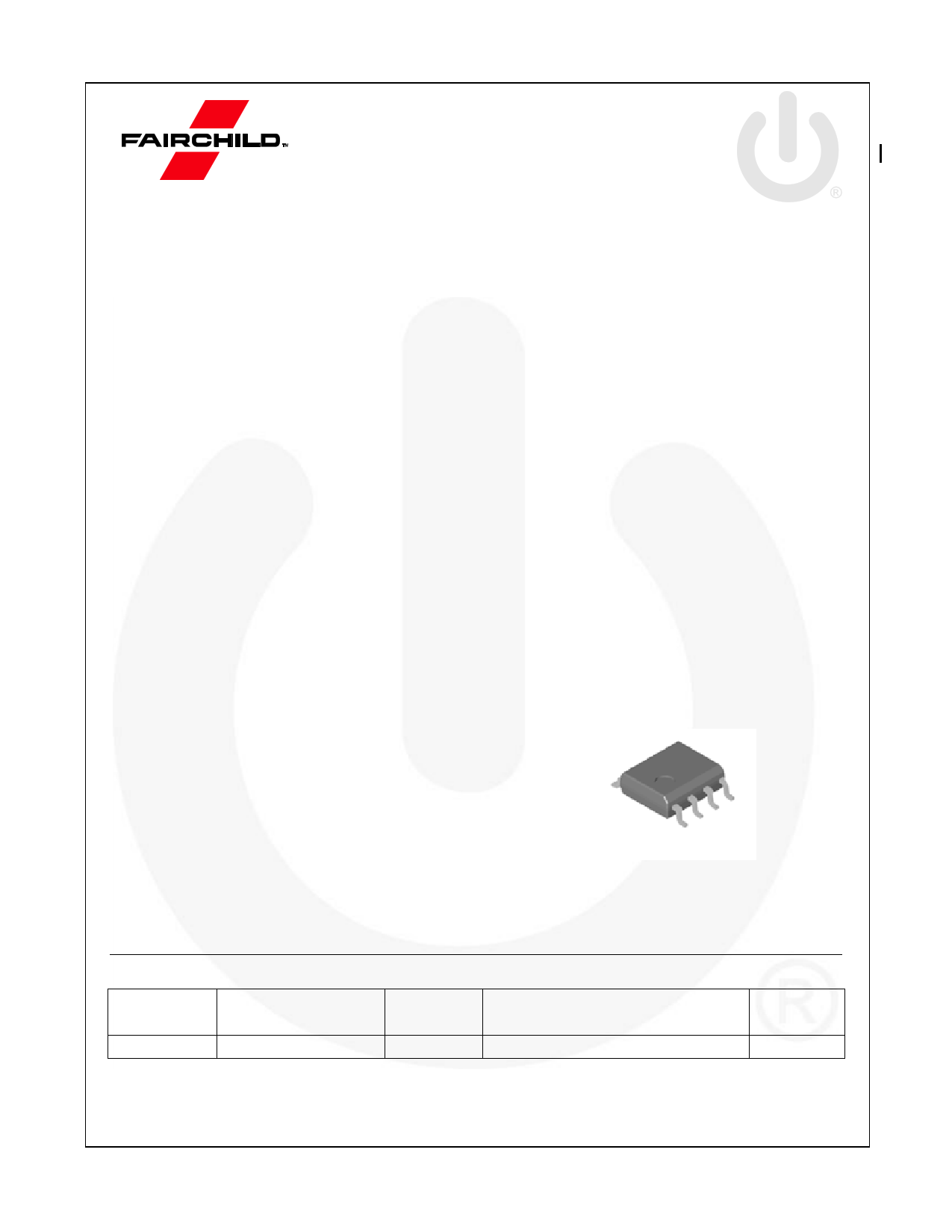
Figure 1. 8-Lead SOIC
Ordering Information
Part Number
Operating
Temperature Range
FL663MX
-40°C to +125°C
Top Mark
FL663
Package
8-Lead, Small-Outline Package (SOIC-8)
Packing
Method
Tape & Reel
© 2015 Fairchild Semiconductor Corporation
FL663 • Rev. 1.0
www.fairchildsemi.com
1 page 
Electrical Characteristics
VDD=15 V and TA=-40°C~125°C unless otherwise noted.
Symbol
Parameter
Conditions
Min. Typ. Max. Unit
VDD Section
VDD-ON Turn-On Threshold Voltage
VDD-OFF Turn-Off Threshold Voltage
IDD-OP
Operating Current
IDD-GREEN Green Mode Operating Supply Current
VDD-OVP VDD Over-Voltage Protection Level
tD-VDDOVP VDD OVP Debounce Time
High Voltage (HV) Section
VHV-MIN Minimum Startup Voltage on HV Pin(3)
IHV Supply Current Drawn from Pin HV
IHV-LC
Leakage Current after Startup
VDL=100 V
HV=500 V,
VDD=VDD-OFF +1 V
15 16 17 V
7.0 7.5 8.0
V
3.2 5.0 mA
0.95 1.20 mA
27 28 29 V
90 200 350 µs
50 V
1.0 2.0 5.0 mA
0.5 3.0 µA
Oscillator Section
Normal
Frequency
Center Frequency
> VO * 0.5, TA=25°C
Frequency Hopping Range
fOSC
Protection
Frequency(4)
Center Frequency
Frequency Hopping Range
< VO * 0.5, TA=25°C
VF-JUM-53
VF-JUM-35
Frequency Jumping Point
50 kHz 33 kHz, VS(3)
33 kHz 50 kHz, VS
fOSC-N-MIN Minimum Frequency at No-Load
fOSC-CM-MIN Minimum Frequency at CCM
VS-F-SKIPH
VS-F-SKIPL
COMV Level for High Cycle Skipping
Period Change(3)
COMV level for Low Cycle Skipping
period Change(3)
△COMV_SKIP
Cycle Skipping Period COMV Hysteresis
Voltage
47
±1.5
1.05
1.28
260
7
50
±2.0
33
±1.3
1.25
1.50
385
12
1.14
0.80
0.34
53
±2.5
1.55
1.75
500
17
kHz
V
V
Hz
kHz
V
V
V
TSKIP-CV
fDV
fDT
Cycle Skipping Period(3)
Frequency Variation vs. VDD Deviation(3)
Frequency Variation vs. Temperature
Deviation
VS-F- SKIPH <COMV<VN
VS-F-SKIPL >COMV
VDD=10~25 V
240
160
12
ms
%
15 %
Voltage Sense (VS) Section
VR
VN
VG
VBIAS-COMV
Reference Voltage for Error AMPs
Green-Mode Starting Voltage on EAV
Green-Mode Ending Voltage on EAV
Adaptive Bias Voltage Dominated by
VCOMV(3)
TA=25°C
fOSC=2 kHz
fOSC=1 kHz
RVS=20 kΩ
2.475
2.500
2.5
0.5
2.525
1.4
V
V
V
V
Continued on the following page…
© 2015 Fairchild Semiconductor Corporation
FL663 • Rev. 1.0
5
www.fairchildsemi.com
5 Page 
Constant Voltage Regulation
During the inductor current discharge time (tDIS), the
sum of output voltage (VO) and diode forward-voltage
drop (VF) is reflected to the auxiliary winding side as
(VO+VF) NA/NS. Since the diode forward-voltage drop
(VF) decreases as current decreases, the auxiliary
winding voltage (VA) reflects the output voltage (VO) at
the end of diode conduction time (tDIS), where the diode
current (IF) diminishes to zero. By sampling the winding
voltage at the end of the diode conduction time (tDIS),
the output voltage (VO) information can be obtained. The
internal error amplifier for output voltage regulation
(EAV) compares the sampled voltage with an internal
precise reference to generate error voltage (VCOMV),
which determines the duty cycle of the MOSFET (Q1) in
Constant Voltage Mode.
Constant Current Regulation
The output current (IO) can be estimated using the peak
drain current (IPK) and inductor current discharge time
(tDIS) since output current (IO) is same as the average of
the diode current (IF_AVG) in steady state. The output
current estimator (IO Estimator) determines the peak
value of the drain current with a peak detection circuit
and calculates the output current (IO) using the inductor
discharge time (tDIS) and switching period (tS). This
output information is compared with an internal precise
reference to generate error voltage (VCOMI), which
determines the duty cycle of the MOSFET (Q1) in
Constant Current Mode. With Fairchild’s innovative
technique TRUECURRENT®, constant current output
can be precisely controlled.
Voltage and Current Error Amplifier
Of the two error voltages, VCOMV and VCOMI, the small
one determines the duty cycle. Therefore, during
Constant Voltage Regulation Mode, VCOMV determines
the duty cycle while VCOMI is saturated to HIGH. During
Constant Current Regulation Mode, VCOMI determines
the duty cycle while VCOMV is saturated to HIGH.
Operating Current
The operating current is typically 3.2 mA. The small
operating current results in higher efficiency and
reduces the VDD capacitor (CVDD) requirement. Once
FL663 enters Green Mode, the operating current is
reduced to 0.95 mA, assisting the power supply in
meeting power conservation requirements.
Green Mode Operation
The FL663 uses voltage regulation error amplifier output
(VCOMV) as an indicator of the output load and modulates
the PWM frequency, as shown in Figure 21. The
switching frequency decreases with cycle skipping as
load decreases. In heavy load conditions, the switching
frequency is fixed at 50 kHz. Once VCOMV decreases
below 2.5 V, the PWM frequency linearly decreases
from 50 kHz. Once VCOMV decreases below VN, the
PWM frequency linearly decreases with cycle skipping
from 50 kHz to reduce switching losses.
fS
50kHz
with cycle skipping
Green
Load
(PFM)
Light & Middle
Load
(PFM + PWM)
Heavy
Load
(PWM)
385Hz
Figure 21.
0.5V
2.5V
VS-F-SKIPL VS-F-SKIPH
VCOMV
Switching Frequency as Output Load
Frequency Hopping
EMI reduction is accomplished by frequency hopping,
which spreads the energy over a wider frequency range
than the bandwidth measured by the EMI test
equipment. FL663 has an internal frequency hopping
circuit that changes the switching frequency between
47 kHz and 53 kHz.
High-Voltage Startup
0 shows the startup block. The HV pin is connected to
the line input or DC link capacitor (CDC). During startup,
the internal startup circuit is enabled. Meanwhile, line
input supplies the current (IStart) to charge the VDD
capacitor (CVDD). When the VDD voltage reaches VDD-ON
(16 V) and VDC is enough high to avoid brownout, the
internal startup circuit is disabled, blocking IStart from
flowing into the HV pin. Once the IC turns on, CVDD is
the only energy source to supply the IC consumption
current before the PWM starts to switch. Thus, CVDD
must be large enough to prevent VDD-OFF (7.5 V) before
the power can be delivered from the auxiliary winding.
To avoid the surge from input source, the RStart is
connected between CDC and HV, with a recommended
value of 100 kΩ.
VLINE
CDL
IStart
HV
+
VDL
-
1
SW1
Brown-Out: ‘H’
Brown-In: ‘L’ Brown-Out
Detector
DVDD
VA
VDD 3
SW2
Internal Bias
CVDD
SW3
16V
+
-
7.5V
SW4
Reset
Normal Operation: ‘H’
OSC Disable: ‘L’
Figure 22. Startup Block
Aux. Winding
VS
4
Protections
The FL663 has several self-protection functions; over-
voltage protection, thermal shutdown protection,
brownout protection, and pulse-by-pulse current limit.
© 2015 Fairchild Semiconductor Corporation
FL663 • Rev. 1.0
11
www.fairchildsemi.com
11 Page | ||
| Páginas | Total 14 Páginas | |
| PDF Descargar | [ Datasheet FL663MX.PDF ] | |
Hoja de datos destacado
| Número de pieza | Descripción | Fabricantes |
| FL663MX | Primary-Side-Regulation PWM Controller | Fairchild Semiconductor |
| Número de pieza | Descripción | Fabricantes |
| SLA6805M | High Voltage 3 phase Motor Driver IC. |
Sanken |
| SDC1742 | 12- and 14-Bit Hybrid Synchro / Resolver-to-Digital Converters. |
Analog Devices |
|
DataSheet.es es una pagina web que funciona como un repositorio de manuales o hoja de datos de muchos de los productos más populares, |
| DataSheet.es | 2020 | Privacy Policy | Contacto | Buscar |