|
|
|
PDF FNA51560T1 Data sheet ( Hoja de datos )
| Número de pieza | FNA51560T1 | |
| Descripción | Motion SPM 55 Series | |
| Fabricantes | Fairchild Semiconductor | |
| Logotipo | ||
Hay una vista previa y un enlace de descarga de FNA51560T1 (archivo pdf) en la parte inferior de esta página. Total 15 Páginas | ||
|
No Preview Available !
FNA51560T1/T3
Motion SPM® 55 Series
June 2014
Features
• UL Certified No. E209204 (UL1557)
• 600 V - 15 A 3-Phase IGBT Inverter Including Control
IC for Gate Drive and Protections
• Low-Loss, Short-Circuit Rated IGBTs
• Separate Open-Emitter Pins from Low-Side IGBTs for
Three-Phase Current Sensing
• Active-HIGH interface, works with 3.3 / 5 V Logic,
Schmitt-trigger Input
• Inter-Lock Function
• HVIC for Gate Driving and Under-Voltage Protection
• HVIC Temperature-Sensing Built-In for Temperature
Monitoring
• Optimized for 5 kHz Switching Frequency
• Isolation Rating: 1500 Vrms / min.
General Description
FNA51560T1/T3 is a Motion SPM 55 module providing a
fully-featured, high-performance inverter output stage for
AC Induction, BLDC, and PMSM motors. These modules
integrate optimized gate drive of the built-in IGBTs to
minimize EMI and losses, while also providing multiple
on-module protection features including under-voltage
lockouts, inter-lock function, over-current shutdown,
thermal monitoring of drive IC, and fault reporting. The
built-in, high-speed HVIC requires only a single supply
voltage and translates the incoming logic-level gate
inputs to the high-voltage, high-current drive signals
required to properly drive the module's robust short-
circuit-rated IGBTs. Separate negative IGBT terminals
are available for each phase to support the widest
variety of control algorithms.
Applications
• Motion Control - Home Appliance / Industrial Motor
Related Resources
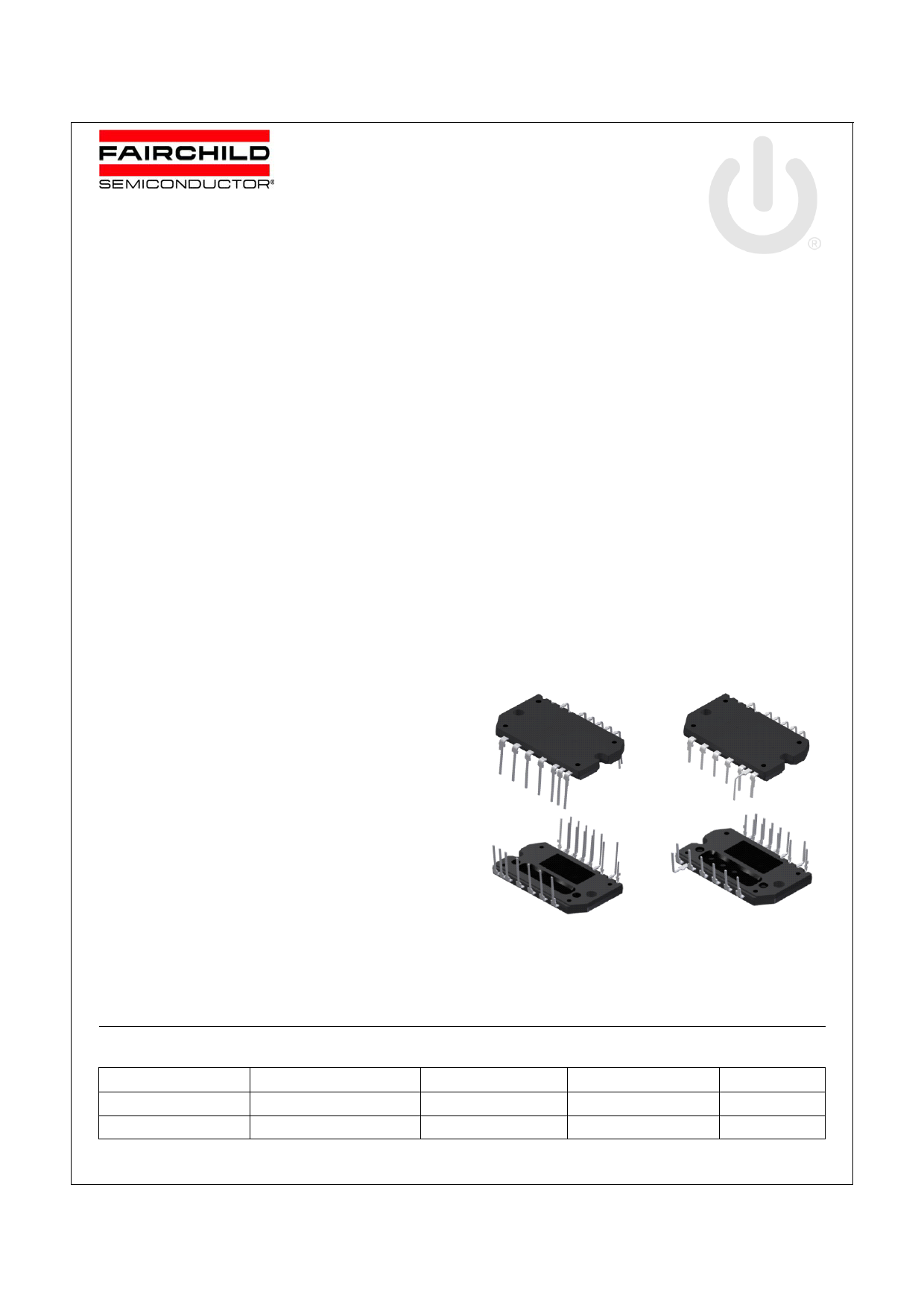
Figure 1. Package Overview
Package Marking and Ordering Information
Device
FNA51560T1
FNA51560T3
Device Marking
FNA51560T1
FNA51560T3
Package
SPMFA-B20
SPMFA-A20
Packing Type
RAIL
RAIL
Quantity
13
13
©2014 Fairchild Semiconductor Corporation
FNA51560T1/T3 Rev. C0
1
www.fairchildsemi.com
1 page 
Absolute Maximum Ratings (TJ = 25°C, unless otherwise specified.)
Inverter Part
Symbol
Parameter
Conditions
VPN
VPN(Surge)
VCES
± IC
± ICP
Supply Voltage
Supply Voltage (Surge)
Collector - Emitter Voltage
Each IGBT Collector Current
Each IGBT Collector Current (Peak)
Applied between P - NU, NV, NW
Applied between P - NU, NV, NW
TC = 25°C, TJ < 150°C
TC = 25°C, TJ < 150°C, Under 1 ms Pulse
Width
PC Collector Dissipation
TJ Operating Junction Temperature
TC = 25°C per Chip
(Note 5)
Note:
5. The maximum junction temperature rating of the power chips integrated within the Motion SPM® 55 product is 150C.
Rating
450
500
600
15
30
27
-40 ~ 150
Unit
V
V
V
A
A
W
°C
Control Part
Symbol
Parameter
VDD Control Supply Voltage
VBS High-Side Control Bias Voltage
VIN Input Signal Voltage
VF Fault Supply Voltage
IF Fault Current
VSC Current Sensing Input Voltage
Conditions
Rating
Applied between VDD - COM
Applied between VB(U) - VS(U), VB(V) - VS(V),
VB(W) - VS(W)
Applied between IN(UH), IN(VH), IN(WH),
IN(UL), IN(VL), IN(WL) - COM
Applied between VF - COM
Sink Current at VF pin
Applied between CSC - COM
20
20
-0.3 ~ VDD +0.3
-0.3 ~ VDD +0.3
5
-0.3 ~ VDD +0.3
Unit
V
V
V
V
mA
V
Total System
Symbol
Parameter
VPN(PROT) Self Protection Supply Voltage Limit
(Short Circuit Protection Capability)
TSTG
VISO
Storage Temperature
Isolation Voltage
Conditions
VDD = VBS = 13.5 ~ 16.5 V
TJ = 150°C, Non-Repetitive, < 2 s
60 Hz, Sinusoidal, AC 1 Minute, Connect
Pins to Heat Sink Plate
Rating
400
-40 ~ 125
1500
Unit
V
°C
Vrms
Thermal Resistance
Symbol
Parameter
Conditions
Min.
Rth(j-c)Q
Rth(j-c)F
Junction to Case Thermal Resistance
Inverter IGBT part (per 1 / 6 module)
Inverter FWD part (per 1 / 6 module)
-
-
Note:
6. For the measurement point of case temperature (TC), please refer to Figure 2.
Typ.
-
-
Max.
4.55
5.4
Unit
°C / W
°C / W
©2014 Fairchild Semiconductor Corporation
FNA51560T1/T3 Rev. C0
5
www.fairchildsemi.com
5 Page 
Lower arms
control input
Protection
Circuit state
Internal IGBT
Gate-Emitter Voltage
Output Current
c1
c6 c7
SET RESET
c4
c3
c2
SC
c8
Sensing Voltage
of the shunt
resistance
Fault Output Signal
SC Reference Voltage
CR circuit time
c5 constant delay
(with the external shunt resistance and CR connection)
c1 : Normal operation: IGBT ON and carrying current.
c2 : Short circuit current detection (SC trigger).
c3 : Hard IGBT gate interrupt.
c4 : IGBT turns OFF.
c5 : Input “L” : IGBT OFF state.
c6 : Input “H”: IGBT ON state, but during the active period of fault output the IGBT doesn’t turn ON.
c7 : IGBT OFF state
Figure 11. Short-Circuit Protection
Hin
Lin
Ho
Lo
Hin : High-side Input Signal
Lin : Low-side Input Signal
Ho : Internal IGBT Gate - Emitter Voltage of High-side
Lo : Internal IGBT Gate - Emitter Voltage of Low-side
Figure 12. Inter-Lock Function
©2014 Fairchild Semiconductor Corporation
FNA51560T1/T3 Rev. C0
11
www.fairchildsemi.com
11 Page | ||
| Páginas | Total 15 Páginas | |
| PDF Descargar | [ Datasheet FNA51560T1.PDF ] | |
Hoja de datos destacado
| Número de pieza | Descripción | Fabricantes |
| FNA51560T1 | Motion SPM 55 Series | Fairchild Semiconductor |
| FNA51560T3 | Motion SPM 55 Series | Fairchild Semiconductor |
| FNA51560TD3 | Motion SPM 55 module | Fairchild Semiconductor |
| Número de pieza | Descripción | Fabricantes |
| SLA6805M | High Voltage 3 phase Motor Driver IC. |
Sanken |
| SDC1742 | 12- and 14-Bit Hybrid Synchro / Resolver-to-Digital Converters. |
Analog Devices |
|
DataSheet.es es una pagina web que funciona como un repositorio de manuales o hoja de datos de muchos de los productos más populares, |
| DataSheet.es | 2020 | Privacy Policy | Contacto | Buscar |