|
|
|
PDF LX1977 Data sheet ( Hoja de datos )
| Número de pieza | LX1977 | |
| Descripción | SMBus Ambient Light Sensor | |
| Fabricantes | Microsemi Corporation | |
| Logotipo | ||
Hay una vista previa y un enlace de descarga de LX1977 (archivo pdf) en la parte inferior de esta página. Total 23 Páginas | ||
|
No Preview Available !
LX1977
TM ® SMBus Ambient Light Sensor
PRODUCTION DATASHEET
DESCRIPTION
The LX1977 is a CMOS based Ambient
Light Sensor (ALS) with an I2C compatible
SMBus interface.
This device is ideal for controlling
display back lighting systems of low cost
consumer products such as TV, portable
computers, handheld devices, or medical
devices. The LX1977 is optimized for a
linear, accurate, and very repeatable input
and output transfer function. The device also
features adjustable input range and gain.
The LX1977 has a spectral response
that emulates the human eye. Specially
designed circuitry produces peak spectral
response at 555 nm, with IR response less
than 10% above 810 nm.
Input dynamic range of this device is
adjustable via SMBus command. It can be set
to either 0 ~ 500 lux, 0 ~ 1000 lux, 0 ~ 2500
lux or 0 ~ 5000 lux.
ALS internal compensation ensures
photodiode dark current are at very low
levels, providing high output accuracy at low
ambient light levels.
The LX1977 integrates a 12-bit Sigma-
Delta A/D converter that converts the ALS
photodiode output into a digital word. This
value is read via the I2C compatible SMBus
interface.
The LX1977 ALS is internally optimized
to an accuracy of approximately 5% over
temperature. The high accuracy and
repeatability of this device eliminates the
need of calibration during product
production, which results in reduced
assembly time and lower production cost.
The LX1977 is available in an 8-pin
MSOP package, and is operational over the
ambient temperature range -40˚C to 85˚C.
KEY FEATURES
Human Eye Spectral Response
Very Low IR Sensitivity
12-bit Resolution
5% Typical Accuracy
Rejection to 50/60Hz
Interference
Programmable Integration Time
Programmable Interrupt Pin
I2C compatible SMBus Interface
Easy Processor Interface
No Optical Filter Needed
APPLICATIONS
Backlight Control for Notebook
Backlight Control for TV
Handheld Devices
Medical Devices
Note: I2C is a trade mark of Philips
PACKAGE ORDER INFO
TA (°C) DU
3 x 5 Glass Top MSOP 8-pin
RoHS Compliant / Pb-free
-40 to 85
LX1977IDU
Note: Available in Tape & Reel. Append the letters “TR” to the part number.
(i.e. LX1977IDU -TR)
THERMAL DATA
θJA = 152 °C/W
THERMAL RESISTANCE-JUNCTION TO AMBIENT
Junction Temperature Calculation: TJ = TA + (PD x θJA).
The θJA numbers are guidelines for the thermal performance of the
device/pc-board system. All of the above assume no ambient airflow.
ABSOLUTE MAXIMUM RATINGS
VDD ............................................................................................................... -0.3 to 6V DC
Input Voltage to All Input Pins ........................................................... -0.3V to VDD + 0.3V
SMBus Pin Voltage (SCL, SDA) .................................................................. -0.3V to 5.5V
SMBus Pin Current (SCL, SDA) ........................................................................... < 10 mA
Operating Temperature Range ........................................................................ -40 to +85°C
Storage Temperature Range.............................................................................-40 to 100°C
RoHS / Pb-free Peak Package Solder Reflow Temperature
(40 seconds maximum exposure).................................................................... 260° (+0, -5)
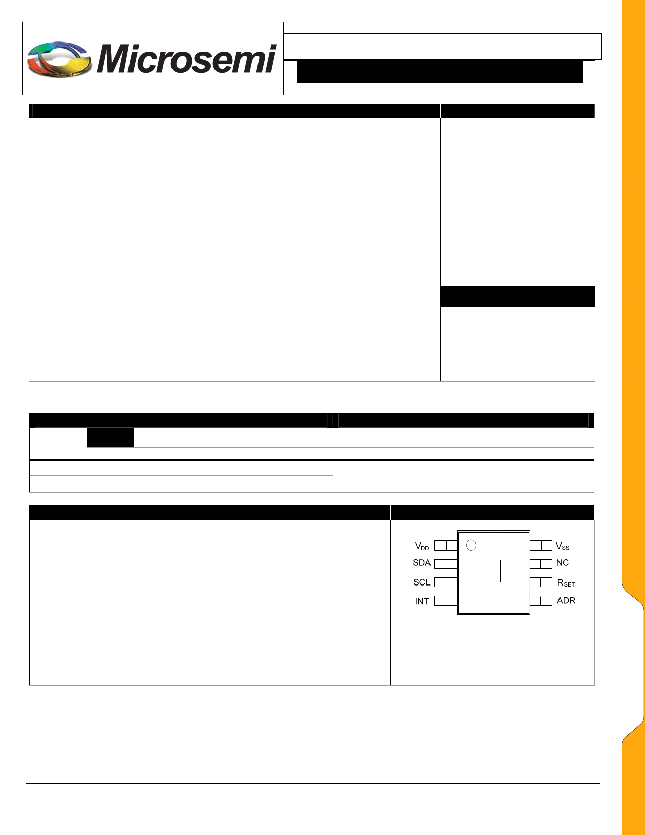
PACKAGE PIN OUT
Notes: Exceeding these ratings could cause damage to the device. All voltages are with respect to
Ground. Currents are positive into, negative out of specified terminal.
GLASS TOP MSOP 8 PIN
(Top View)
RoHS / Pb-free 100% Matte Tin
Copyright © 2010
Rev. 1.0, 2010-03-25
Microsemi
Analog Mixed Signal Group
11861 Western Avenue, Garden Grove, CA. 92841, 714-898-8121, Fax: 714-893-2570
Page 1
1 page 
LX1977
TM ® SMBus Ambient Light Sensor
PRODUCTION DATASHEET
APPLICATION NOTE
BASIC FUNCTIONALITY
The LX1977 is an ALS with an I2C compatible SMBus
interface. It contains a high sensitivity close to human eye
response photodiode, a 12-bit Sigma-Delta ADC and a SMBus
interface. The Sigma-Delta ADC converts photodiode current to
digital values that correspond to the light incident on the
photodiode. The integrating nature of the ADC allows the device
to reject 50Hz and 60Hz flicker noise from environmental
lighting.
The Sigma-Delta ADC provides the flexibility to set different
conversion times, or integration time. It has four conversion
time selections to meet different application requirements. The
clock source for the ADC is also selectable from either an
internal clock or a SMBus clock. For internal clock selection,
the device features full speed (40.96kHz) and quarter speed
(10.24kHz) selection. The ADC conversion result is stored in a
12-bit register for read back even when another conversion is in
process.
SMBus INTERFACE
LX1977 is a nine-register device which uses SMBus or I2C
protocols to communicate with the host system. All registers
are defined as full byte wide. Some registers contain reserved
(undefined) bits with a default value of “0”, or are read only bits
that are status indicators. Six of the nine registers are capable of
both read and write, and three registers are read only. See the
LX1977 Register Definitions section for details.
The LX1977 communicates over the SMBus and operates in
a “slave” mode receiving commands and sending / receiving
data to / from the host or “master”. Only standard two-wire
SMBus and I2C compatible serial bus and protocols may be
used for this device. The LX1977 can be configured for one of
the three addresses by connecting the ADR input pin to ground,
VDD, or simply leaving it OPEN.
In this document, the device address is always expressed as
full 8 bit address. The high nibble of the address is from bit 7 to
bit 4. In the low nibble, bit 0 is always the R/W bit and in 8 bit
address format it is considered 0.
The address could be changed dynamically. The requirement is
that after the change, the LX1977 ALS should be disabled and
then enabled either via bit 6 of register 00h or a VDD power cycle.
Table 2: Address = 20h
1 7 11 8
S Slave Address Wr A
Data Byte
0010000
0
Table 3: Address = 22h
1 7 11 8
S Slave Address Wr A
Data Byte
0010001
0
Table 4: Address = 70h
1 7 11 8
S Slave Address Wr A
Data Byte
0111000
0
11
AP
11
AP
11
AP
SMBus PROTOCOL
The only required command protocols are SMBus Send Byte,
Receive Byte, Read Byte / Word, and the Write Byte / Word
protocols. See Table 7 ~ Table 12 for details.
Writes to registers can be performed by either the SMBus
Write Byte / Word protocols and / or by internal IC logic,
depending on the register type (see Table 13). Send Byte
protocol can only be used on the Command / Status register
(register 00h).
Table 1: Address strapping codes
Option #
1
2
3
ADR
GND
OPEN
VDD
Hex Address
20h
22h
70h
Read can be performed on all registers by issuing the Read
Byte / Word protocol. Note that Receive Byte protocol can only
be used on the Command / Status register (register 00h) for a
quick test of the status bits. Read Only registers can be written
only by internal logics. Their contents will not be affected by
SMBus write commands.
When LX1977 is initially powered, it will first test the
address selection pin input to determine its own address and then
look for its unique address each time it detects a “Start
Condition”. If the address does not match, the LX1977 ignores
all bus activity until it encounters another “Start Condition”. If
the address is a match, the LX1977 acknowledges that it has
detected its address and a W/R bit to either read or write. If the
Copyright © 2010
Rev. 1.0, 2010-03-25
Microsemi
Analog Mixed Signal Group
11861 Western Avenue, Garden Grove, CA. 92841, 714-898-8121, Fax: 714-893-2570
Page 5
5 Page 
LX1977
TM ® SMBus Ambient Light Sensor
PRODUCTION DATASHEET
Set ADC to continuous conversion mode and start conversion. ADC_FLAG indicates
conversion status, 0 means conversion is in process, 1 means previous conversion is done
1
1
and data is ready in register 07h and 08h. Actually, after the first conversion, this bit will be
always 1. Interrupt function applies to this mode.
Note: When this mode is set, the ADC_FLAG will be set to zero right away.
ADC_CLK (bit 3, R / W): Selects the internal ADC clock speed when CLK_SEL (bit 7) of register 01h is 0
= 0, select clock speed to normal (40.96 kHz)
= 1, select clock speed to ¼ normal (10.24 kHz)
When clock speed is selected, the selectable integration time set will be determined automatically.
For example, when ADC_CLK = 1, the selectable integration time will be 25ms, 100ms, 200ms or
400ms. Please refer to Table 24 for details.
INT_FLAG (bit 2, R / W): Interrupt Status Report
= 0, no interrupt or was cleared. This bit can be set to 1 or 0 by SMBus command. Setting zero
to this bit will set the INT pin to high regardless of the previous state. When it is set to zero,
the internal counter for INT_PERSIST_CTRL will be reset to 0.
= 1, interrupt triggered. When this bit is 1 and INT_ENA = 1, the INT pin will be asserted low
and stay low until this bit is set to zero or INT_ENA = 0. Writing 1 to this bit will override
any internal setting and generate an interrupt if INT_ENA = 1. This function is useful for
testing user hardware and debugging software.
Note:
ADC will continue to run regardless of the interrupt status unless it is stopped by setting START_ADC
bit to 0. Note that the ADC integration time is much longer than the interrupt response time. Data output
of the ADC that generated the interrupt must be read immediately as the next sampled data by the ADC
will write over the DCOUNT register during continuous conversion mode.
INT_ENA (bit 1, R / W): Interrupt Enable Bit
= 0, Disable interrupt pin function
= 1, Enable interrupt pin function
Note:
(1) When INT_ENA = 0, the INT pin function will be disabled. However, the INT_FLAG function
could still be used as software interrupt to monitor the ALS readings. The user can still set the
thresholds and read the INT_FLAG status periodically or when it is needed instead of reading the
ALS data and calculating. If the INT_FLAG = 1, then it means the ALS reading is outside the
boundaries. If this function is not needed, the user just simply ignores the INT_FLAG bit status.
(2) When INT_ENA = 1, the INT pin will perform the normal interrupt function.
(3) When ALS_ENA = 0, the INT pin will be set to high regardless of its previous status.
OV (bit 0, R): Overflow Indicator.
= 0, if DCOUNT has reached the maximum value and this bit is still 0, it means that the input light has
reached the maximum range but not over.
= 1, 1 on this bit indicates that the DCOUNT has reached the maximum value and the input light is over the
selected range limit. Bigger range should be selected.
Table 16: Maximum Count for Different TINT Time
Full Scale ADC Output Value
@ FOSC= 40.96kHz,
RANGE_SEL = 00b (0 ~ 500 lux)
DCOUNT
DCOUNT
TINT = 100 ms
TINT = 50 ms
4095
2047
Counts
Copyright © 2010
Rev. 1.0, 2010-03-25
Microsemi
Analog Mixed Signal Group
11861 Western Avenue, Garden Grove, CA. 92841, 714-898-8121, Fax: 714-893-2570
Page 11
11 Page | ||
| Páginas | Total 23 Páginas | |
| PDF Descargar | [ Datasheet LX1977.PDF ] | |
Hoja de datos destacado
| Número de pieza | Descripción | Fabricantes |
| LX1970 | Visible Light Sensor | Microsemi Corporation |
| LX1971 | Wide Range Visible Light Sensor | Microsemi Corporation |
| LX1972 | Ambient Light Detector | Microsemi Corporation |
| LX1972A | Ambient Light Detector | Microsemi Corporation |
| Número de pieza | Descripción | Fabricantes |
| SLA6805M | High Voltage 3 phase Motor Driver IC. |
Sanken |
| SDC1742 | 12- and 14-Bit Hybrid Synchro / Resolver-to-Digital Converters. |
Analog Devices |
|
DataSheet.es es una pagina web que funciona como un repositorio de manuales o hoja de datos de muchos de los productos más populares, |
| DataSheet.es | 2020 | Privacy Policy | Contacto | Buscar |