|
|
|
PDF LTC6752-4 Data sheet ( Hoja de datos )
| Número de pieza | LTC6752-4 | |
| Descripción | 2.9ns Comparator Family | |
| Fabricantes | Linear Technology | |
| Logotipo | ||
Hay una vista previa y un enlace de descarga de LTC6752-4 (archivo pdf) en la parte inferior de esta página. Total 30 Páginas | ||
|
No Preview Available !
LTC6752/LTC6752-1/
LTC6752-2/LTC6752-3/LTC6752-4
280MHz, 2.9ns Comparator
Family with Rail-to-Rail Inputs
and CMOS Outputs
FEATURES
nn Very High Toggle Rate: 280MHz
nn Low Propagation Delay: 2.9ns
nn Rail-to-Rail Inputs Extend Beyond Both Rails
nn Output Current Capability: ±22mA
nn Low Quiescent Current: 4.5mA
nn Features within the LTC6752 Family:
nn 2.45V to 5.25V Input Supply and 1.71V to 3.5V
Output Supply (Separate Supply Option)
nn 2.45V to 3.5V Supply (Single Supply Option)
nn Shutdown Pin for Reduced Power
nn Output Latch and Adjustable Hysteresis
nn Complementary Outputs
nn Packages: TSOT-23, SC70, MSOP, 3mm × 3mm QFN
nn Direct Replacement for ADCMP60X Family
nn Operating Temperature Range: –40°C to 125°C
APPLICATIONS
nn Clock and Data Recovery
nn Level Shifting
nn High Speed Data Acquisition Systems
nn Window Comparators
nn High Speed Line Receivers
nn Fast Crystal Oscillators
nn Time of Flight Measurements
nn Time Domain Reflectometry
DESCRIPTION
The LTC®6752 is a family of very high speed comparators
capable of supporting toggle rates up to 280MHz. These
comparators exhibit low propagation delays of 2.9ns, and
fast rise/fall times of 1.2ns. There are a total of 5 members
in the LTC6752 family, with different options for separate
input and output supplies, shutdown, output latch, adjust-
able hysteresis, complementary outputs, and package.
The LTC6752 comparators have rail-to-rail inputs that
operate from 2.45V, up to 3.5V or 5.25V, depending on
the option. The outputs are CMOS and the separate supply
options can operate down to 1.71V, allowing for directly
interfacing to 1.8V logic devices.
The low propagation delay of only 2.9ns combined with
low dispersion of only 1.8ns (10mV to 125mV overdrive
variation) makes these comparators an excellent choice
for critical timing applications. Similarly, the fast toggle
rate and the low jitter of 4.5ps RMS (100mVP-P, 100MHz
input) make the LTC6752 family ideally suited for high
frequency line driver and clock recovery circuits.
L, LT, LTC, LTM, Linear Technology and the Linear logo are registered trademarks of Linear
Technology Corporation. All other trademarks are the property of their respective owners.
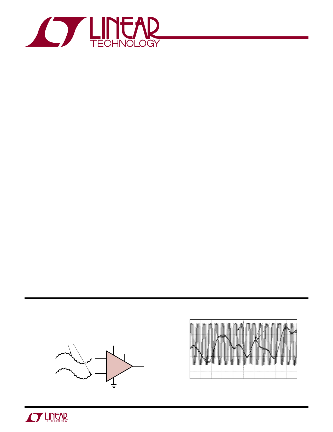
TYPICAL APPLICATION
High Speed Differential Line Receiver with Excellent
Common Mode Rejection
SMALL DIFFERENTIAL SIGNAL WITH
LARGE COMMON MODE COMPONENT
VCC = 5V
+IN +
VDD = 2.7V
LTC6752-2
Q
–IN –
VEE
6752 T01a
500mV/DIV
Q –IN +IN
50ns/DIV
6752 T01a
For more information www.linear.com/LTC6752
6752fa
1
1 page 
LTC6752/LTC6752-1/
LTC6752-2/LTC6752-3/LTC6752-4
E LECTRICAL CHARACTERISTICS (VCC = 2.5V, VDD = 2.5V, VEE = 0). The l denotes the specifications which
apply over
VOVERDRIVE
the specified
= 50mV, –IN
=teVmCpMer=a3tu0r0emraVn,g+eIN, o=th–eINrw+isVeOsVpEeRcDiRfiIVcEa,ti1o5n0smaVresatet pTAsi=ze25u°nCle.sLsEo/HthYeSrTw,isSeHnDoNtepdi.ns
floating,
CL
=
5pF,
SYMBOL PARAMETER
CONDITIONS
MIN TYP MAX UNITS
Latching/Adjustable Hysteresis Characteristics (LTC6752-1/LTC6752-2/LTC6752-3 Only)
VLE/HYST
LE/HYST Pin Voltage
RHYST
Resistance Looking Into LE/HYST
VHYST_LARGE Hysteresis Voltage
VIL_LE
Latch Pin Voltage, Latch Guaranteed
VIH_LE
Latch Pin Voltage, Hysteresis Disabled
IIH_LE
Latch Pin Current High
IIL_LE
Latch Pin Current Low
tSETUP
Latch Setup Time (Note 10)
tHOLD
Latch Hold Time (Note 10)
tPL Latch to Output Delay
Shutdown Characteristics (LTC6752-2/LTC6752-3 Only)
Open Circuit
LE/HYST Pin Voltage < Open Circuit Value
VLE/HYST = 800mV
Output Not Latched
VLE/HYST = 1.7V
VLE/HYST = 0.3V
1.05 1.25 1.45
l 15 20 25
40
l 0.3
l 1.7
l 30 72
l –70
–47
–2
2
7
V
kΩ
mV
V
V
µA
µA
ns
ns
ns
ISD_VCC
Shutdown Mode Input Stage Supply Current VSHDN = 0.6V
400 585
µA
l 620 µA
ISD_VDD
Shutdown Mode Output Stage Supply
Current
VSHDN = 0.6V, LTC6752-2
185 340
µA
l 380 µA
VSHDN = 0.6V, LTC6752-3
250 650
µA
l 680 µA
tSD
VIH_SD
VIL_SD
tWAKEUP
Shutdown Time
Shutdown Pin Voltage High
Shutdown Pin Voltage Low
Wake-Up Time from Shutdown
Output Hi-Z
Part Guaranteed to Be Powered On
Part Guaranteed to Be Powered Off
VOD = 100mV, Output Valid
80
l 1.3
l 0.6
100
ns
V
V
ns
(VCC = 3.3V, VDD = 3.3V, VEE = 0). The l denotes the specifications which apply over the specified temperature range, otherwise
sVpOeVcEiRfDicRaIVtiEo,n1s5a0rmeVatsTteAp=s2iz5e°Cun. lLeEs/sHoYtShTe,rwSHisDeNnoptiends.floating, CL = 5pF, VOVERDRIVE = 50mV, –IN = VCM = 300mV, +IN = –IN +
SYMBOL PARAMETER
CONDITIONS
MIN TYP MAX UNITS
VCC - VEE Supply Voltage (Note 5)
LTC6752/LTC6752-1 (Total Supply)
l 2.45
LTC6752-2/LTC6752-3/LTC6752-4 (Input Stage) l 2.45
3.5 V
5.25 V
VDD - VEE
VCMR
VOS
Output Supply Voltage (Note 5)
Input Voltage Range (Note 7)
Input Offset Voltage (Note 6)
LTC6752-2/LTC6752-3/LTC6752-4
l 1.71
3.5
l VEE – 0.2
VCC + 0.1
–5.5
l –9
±1.2
5.5
9
V
V
mV
mV
TCVOS
VHYST
CIN
RDM
RCM
IB
Input Offset Voltage Drift
Input Hysteresis Voltage (Note 6)
Input Capacitance
Differential Mode Resistance
Common Mode Resistance
Input Bias Current
LE/HYST Pin Floating
VCM = VEE + 0.3V
l
–3.8
l –4.1
18
4.7
1.1
57
6.4
–1.4
µV/°C
mV
pF
kΩ
MΩ
µA
µA
VCM = VCC – 0.3V
0.33 1.5
µA
l 2.3 µA
IOS Input Offset Current
l –0.75 ±0.1 0.75
µA
For more information www.linear.com/LTC6752
6752fa
5
5 Page 
LTC6752/LTC6752-1/
LTC6752-2/LTC6752-3/LTC6752-4
T YPICAL PERFORMANCE CHARACTERISTICS DC VCC = VDD = 2.5V, CLOAD = 5pF,
VOVERDRIVE = 50mV, VCM = 300mV,TA = 25°C unless otherwise noted. VCC ≠ VDD conditions applicable only to the LTC6752-2/ LTC6752-3/
LTC6752-4.
Output Short-Circuit Current vs
Temperature
80
60
SINKING
40
20
0
SOURCING
–20
–40 VCC = 5V, VDD = 1.8V
–60
VCC = VDD = 2.5V
VCC = VDD = 3.3V
–80
–55 –35 –15 5 25 45 65 85 105 125
TEMPERATURE (°C)
6752 G10
Output Low Voltage vs Load
Current
4.5
MEASURED FROM VEE
4.0
3.5
VCC = 3.3V
VDD = 3.3V
3.0
VCC = 2.5V
2.5 VDD = 2.5V
2.0
1.5
VCC = 5V
VDD = 1.8V
1.0
0.5
0
0 5 10 15 20 25 30 35 40 45
SINKING CURRENT (mA)
6752 G11
Output High Voltage vs Sourcing
Current
0
–0.5
VCC = 3.3V
VDD = 3.3V
–1.0
–1.5
–2.0
VCC = 5V
VDD = 1.8V
–2.5
VCC = 2.5V
VDD = 2.5V
–3.0
–3.5
–4.0
–4.5
0
10 20 30 40 50 60 70 80
SOURCING CURRENT (mA)
6752 G12
Output High/Low Voltage vs
Temperature
300 SOURCE/SINK CURRENT = 8mA
250
200 VOL
MEASURED
FROM VEE
Supply Current vs Temperature
(LTC6752/LTC6752-1/LTC6752-2/
LTC6752-4)
5.0
4.5
4.0
ITOTAL (LTC6752-2/LTC6752-4)
ICC (LTC6752/LTC6752-1)
3.5
Supply Current vs Temperature
(LTC6752-3)
7
6
ITOTAL
5
150 3.0
100
VOH
MEASURED
FROM VDD
2.5
2.0
50 1.5
IVDD (LTC6752-2/LTC6752-4)
IVCC (LTC6752-2/LTC6752-4)
4
3
2
IVDD
IVCC
0
–55 –35 –15 5 25 45 65 85 105 125
TEMPERATURE (°C)
6752 G13
Supply Current vs Supply Voltage
(LTC6752/LTC6752-1/LTC6752-2/
LTC6752-4)
6 VCC = VDD
5
4
ITOTAL (LTC6752-2/LTC6752-4)
ICC (LTC6752/LTC6752-1)
3
IVDD (LTC6752-2/LTC6752-4)
2
IVCC (LTC6752-2/LTC6752-4)
1
1.0
–55 –35 –15 5 25 45 65 85 105 125
TEMPERATURE (°C)
6752 G14
Supply Current vs Supply Voltage
(LTC6752-3)
8 VCC = VDD
7
6 ITOTAL
5
4 IVDD
3
2 IVCC
1
1
–55 –35 –15 5 25 45 65 85 105 125
TEMPERATURE (°C)
6752 G15
Supply Current vs Input Common
Mode Voltage (LTC6752/LTC6752-1/
LTC6752-2/LTC6752-4)
4.85
4.80
4.75
4.70
4.65
4.60
4.55
4.50
0
2.45
2.75 3.05 3.35
SUPPLY VOLTAGE (V)
3.65
6752 G16
0
2.45
2.75 3.05 3.35
SUPPLY VOLTAGE (V)
3.65
6752 G17
4.45
–0.2
0.5 1.2 1.9 2.6
INPUT COMMON MODE VOLTAGE (V)
6752 G18
6752fa
For more information www.linear.com/LTC6752
11
11 Page | ||
| Páginas | Total 30 Páginas | |
| PDF Descargar | [ Datasheet LTC6752-4.PDF ] | |
Hoja de datos destacado
| Número de pieza | Descripción | Fabricantes |
| LTC6752-1 | 2.9ns Comparator Family | Linear Technology |
| LTC6752-2 | 2.9ns Comparator Family | Linear Technology |
| LTC6752-3 | 2.9ns Comparator Family | Linear Technology |
| LTC6752-4 | 2.9ns Comparator Family | Linear Technology |
| Número de pieza | Descripción | Fabricantes |
| SLA6805M | High Voltage 3 phase Motor Driver IC. |
Sanken |
| SDC1742 | 12- and 14-Bit Hybrid Synchro / Resolver-to-Digital Converters. |
Analog Devices |
|
DataSheet.es es una pagina web que funciona como un repositorio de manuales o hoja de datos de muchos de los productos más populares, |
| DataSheet.es | 2020 | Privacy Policy | Contacto | Buscar |