|
|
PDF K4T1G084QR Data sheet ( Hoja de datos )
| Número de pieza | K4T1G084QR | |
| Descripción | 1Gb R-die DDR2 SDRAM | |
| Fabricantes | Samsung semiconductor | |
| Logotipo | ||
Hay una vista previa y un enlace de descarga de K4T1G084QR (archivo pdf) en la parte inferior de esta página. Total 30 Páginas | ||
|
No Preview Available !
K4T1G084QR
DDR2 SDRAM
1Gb R-die DDR2 SDRAM Specification
60FBGA with Lead-Free & Halogen-Free
(RoHS compliant)
INFORMATION IN THIS DOCUMENT IS PROVIDED IN RELATION TO SAMSUNG PRODUCTS,
AND IS SUBJECT TO CHANGE WITHOUT NOTICE.
NOTHING IN THIS DOCUMENT SHALL BE CONSTRUED AS GRANTING ANY LICENSE,
EXPRESS OR IMPLIED, BY ESTOPPEL OR OTHERWISE,
TO ANY INTELLECTUAL PROPERTY RIGHTS IN SAMSUNG PRODUCTS OR TECHNOLOGY. ALL
INFORMATION IN THIS DOCUMENT IS PROVIDED
ON AS "AS IS" BASIS WITHOUT GUARANTEE OR WARRANTY OF ANY KIND.
1. For updates or additional information about Samsung products, contact your nearest Samsung office.
2. Samsung products are not intended for use in life support, critical care, medical, safety equipment, or similar
applications where Product failure couldresult in loss of life or personal or physical harm, or any military or
defense application, or any governmental procurement to which special terms or provisions may apply.
* Samsung Electronics reserves the right to change products or specification without notice.
www.BDTIC.1cofo42 m/SAMSUNG Rev. 1.1 July 2008
1 page 
K4T1G084QR
3.0 Package Pinout/Mechanical Dimension & Addressing
DDR2 SDRAM
3.1 x8 package pinout (Top View) : 60ball FBGA Package
1 23
7 89
VDD
DQ6
NU/
RDQS
VSSQ
VSS
DM/
RDQS
VDDQ DQ1 VDDQ
A
B
C
VSSQ DQS VDDQ
DQS VSSQ DQ7
VDDQ DQ0 VDDQ
DQ4 VSSQ DQ3 D DQ2 VSSQ DQ5
VDDL VREF VSS
E VSSDL CK
VDD
CKE WE F RAS CK ODT
BA2 BA0 BA1 G CAS CS
A10/AP A1 H A2 A0 VDD
VSS
A3
A5 J
A6
A4
A7 A9 K A11 A8 VSS
VDD A12 NC L NC A13
Note:
1. Pins B3 and A2 have identical capacitance as pins B7 and A8.
2. For a read, when enabled, strobe pair RDQS & RDQS are identical in
function and timing to strobe pair DQS & DQS and input masking function
is disabled.
3. The function of DM or RDQS/RDQS are enabled by EMRS command.
4. VDDL and VSSDL are power and ground for the DLL.
Ball Locations (x8)
: Populated Ball
+ : Depopulated Ball
Top View (See the balls through the Package)
123456789
A
B
C
D
E
F+
G
H+
J
K+
L
+ ++
+ ++
+ ++
+ ++
+ ++
+ ++
+ ++
+ ++
+ ++
+ ++
+ ++
+
+
+
www.BDTIC.5cofo42 m/SAMSUNG Rev. 1.1 July 2008
5 Page 
K4T1G084QR
DDR2 SDRAM
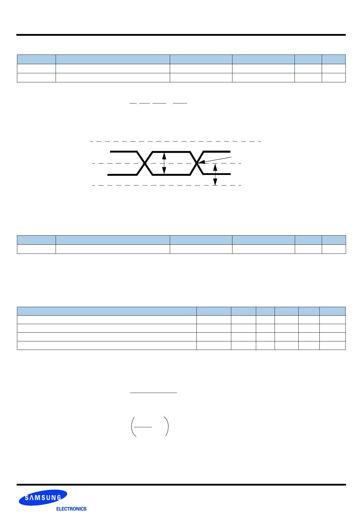
7.6 Differential input AC logic Level
Symbol
VID(AC)
VIX(AC)
Parameter
AC differential input voltage
AC differential cross point voltage
Min.
0.5
0.5 * VDDQ - 0.175
Max.
VDDQ + 0.6
0.5 * VDDQ + 0.175
Units
V
V
Notes
1
2
Note :
1. VID(AC) specifies the input differential voltage |VTR -VCP | required for switching, where VTR is the true input signal (such as CK, DQS, LDQS or UDQS)
and VCP is the complementary input signal (such as CK, DQS, LDQS or UDQS). The minimum value is equal to V IH (AC) - V IL(AC).
2. The typical value of VIX(AC) is expected to be about 0.5 * VDDQ of the transmitting device and VIX(AC) is expected to track variations in VDDQ .
VIX(AC) indicates the voltage at which differential input signals must cross.
VDDQ
VTR
VCP
VID
Crossing point
VIX or VOX
VSSQ
< Differential signal levels >
7.7 Differential AC output parameters
Symbol
VOX(AC)
Parameter
AC differential cross point voltage
Min.
0.5 * VDDQ - 0.125
Max.
0.5 * VDDQ + 0.125
Units
V
Note
1
Note :
1. The typical value of VOX(AC) is expected to be about 0.5 * VDDQ of the transmitting device and VOX(AC) is expected to track variations in VDDQ .
VOX(AC) indicates the voltage at which differential output signals must cross.
8.0 ODT DC electrical characteristics
PARAMETER/CONDITION
Rtt effective impedance value for EMRS(A6,A2)=0,1; 75 ohm
Rtt effective impedance value for EMRS(A6,A2)=1,0; 150 ohm
Rtt effective impedance value for EMRS(A6,A2)=1,1; 50 ohm
Deviation of VM with respect to VDDQ/2
Note : Test condition for Rtt measurements
SYMBOL
Rtt1(eff)
Rtt2(eff)
Rtt3(eff)
delta VM
MIN NOM MAX UNITS NOTES
60 75 90 ohm
1
120 150 180 ohm
1
40 50 60 ohm
1
-6
+6 %
1
Measurement Definition for Rtt(eff): Apply VIH (ac) and VIL (ac) to test pin separately, then measure current I(VIH (ac)) and I( VIL (ac)) respectively. VIH
(ac), VIL (ac), and VDDQ values defined in SSTL_18
Rtt(eff) = VIH (ac) - VIL (ac)
I(VIH (ac)) - I(VIL (ac))
delta VM =
2 x Vm
- 1 x 100%
VDDQ
Measurement Definition for VM: Measure voltage (VM) at test pin (midpoint) with no load.
www.BDTIC.com/SAMSUNG11 of 42
Rev. 1.1 July 2008
11 Page | ||
| Páginas | Total 30 Páginas | |
| PDF Descargar | [ Datasheet K4T1G084QR.PDF ] | |
Hoja de datos destacado
| Número de pieza | Descripción | Fabricantes |
| K4T1G084QA-ZCE6 | 1Gb A-die DDR2 SDRAM Specification | Samsung semiconductor |
| K4T1G084QC | (K4T1G044QC / K4T1G084QC) 1Gb C-die DDR2 SDRAM Specification | Samsung semiconductor |
| K4T1G084QD | (K4T1G084QD / K4T1G164QD) 1Gb A-die DDR2 SDRAM Specification | Samsung semiconductor |
| K4T1G084QE | 1Gb E-die DDR2 SDRAM | Samsung Electronics |
| Número de pieza | Descripción | Fabricantes |
| SLA6805M | High Voltage 3 phase Motor Driver IC. |
Sanken |
| SDC1742 | 12- and 14-Bit Hybrid Synchro / Resolver-to-Digital Converters. |
Analog Devices |
|
DataSheet.es es una pagina web que funciona como un repositorio de manuales o hoja de datos de muchos de los productos más populares, |
| DataSheet.es | 2020 | Privacy Policy | Contacto | Buscar |
