|
|
|
PDF L6569AD Data sheet ( Hoja de datos )
| Número de pieza | L6569AD | |
| Descripción | HIGH VOLTAGE HALF BRIDGE DRIVER WITH OSCILLATOR | |
| Fabricantes | STMicroelectronics | |
| Logotipo | ||
Hay una vista previa y un enlace de descarga de L6569AD (archivo pdf) en la parte inferior de esta página. Total 13 Páginas | ||
|
No Preview Available !
L6569
L6569A
HIGH VOLTAGE HALF BRIDGE
DRIVER WITH OSCILLATOR
s HIGH VOLTAGE RAIL UP TO 600V
s BCD OFF LINE TECHNOLOGY
s INTERNAL BOOTSTRAP DIODE
STRUCTURE
s 15.6V ZENER CLAMP ON VS
s DRIVER CURRENT CAPABILITY:
- SINK CURRENT = 270mA
- SOURCE CURRENT = 170mA
s VERY LOW START UP CURRENT: 150µA
s UNDER VOLTAGE LOCKOUT WITH
HYSTERESIS
s PROGRAMMABLE OSCILLATOR
FREQUENCY
s DEAD TIME 1.25µs
s dV/dt IMMUNITY UP TO ±50V/ns
s ESD PROTECTION
DESCRIPTION
The device is a high voltage half bridge driver with
built in oscillator. The frequency of the oscillator can
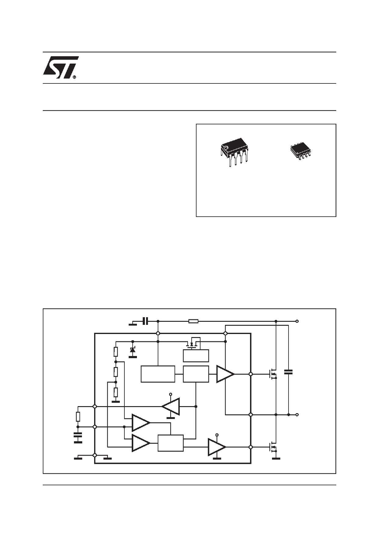
BLOCK DIAGRAM
Minidip
SO8
ORDERING NUMBERS:
L6569
L6569D
L6569A
L6569AD
be programmed using external resistor and capaci-
tor. The internal circuitry of the device allows it to be
driven also by external logic signal.
The output drivers are designed to drive external n-
channel power MOSFET and IGBT. The internal log-
ic assures a dead time [typ. 1.25µs] to avoid cross-
conduction of the power devices.
Two version are available: L6569 and L6569A. They
differ in the low voltage gate driver start up sequence.
RF 2
RF CF 3
CF
GND 4
CVS
1
VS RHV BOOT
8
Source
CHARGE
PUMP
BIAS
REGULATOR
LEVEL
SHIFTER
7 HVG
VS
BUFFER
HIGH
SIDE
DRIVER
6
OUT
COMP
COMP
LOGIC
VS
LOW SIDE
DRIVER
5
LVG
H.V.
CBOOT
LOAD
D94IN058D
June 2000
This is preliminary information on a new product now in development. Details are subject to change without notice.
1/13
1 page 
L6569 L6569A
Bootstrap Function
The L6569 has an internal Bootstrap structure that enables the user to avoid the external diode needed, in sim-
ilar devices, to perform the charge of the bootstrap capacitor that, in turns, provide an appropriate driving to the
Upper External Mosfet.
The operation is achieved with an unique structure (patented) that uses a High Voltage Lateral DMOS driven
by an internal charge pump (see Block Diagram) and synchronized, with a 50 nsec delay, with the Low Side
Gate driver (LVG pin), actually working as a synchronous rectifier .
The charging path for the Bootstrap capacitor is closed via the Lower External Mosfet that is driven ON (i.e. LVG
High) for a time interval:
TC = RF · CF · In2 → 1.1 · RF · CF
starting from the time the Supply Voltage VS has reached the Turn On Voltage (VSUVP = 9 V typical value).
After time T1 (see waveform Diagram) the LDMOS that charges the Bootstrap Capacitor, is on with a RON=120Ω
(typical value).
In the L6569A a different start up procedure is followed (see waveform Diagram). The Lower External Mosfet is
drive OFF until VS has reached the Turn On Threshold (VSUVPp), then again the TC time interval starts as above.
Being the LDMOS used to implement the bootstrap operation a ”bi-directional” switch the current flowing into
the BOOT pin (pin 8) can lead an undue stress to the LDMOS itself if a ZERO VOLTAGE SWITCHING opera-
tions is not ensured, and then an high voltage is applied to the BOOT pin. This condition can occur, for example,
when the load is removed and an high resistive value is placed in series with the gate of the external Power
Mos. To help the user to secure his design a SAFE OPERATING AREA for the Bootstrap LDMOS is provided
(fig. 7).
Let’s consider the steps that should be taken.
1) Calculate the Turn on delay ( td ) of your Lower Power MOS:
td
=
(Rg + Rid ) ⋅ Ciss ⋅ ln
---------1-----------
1 – V-----T---H--
VS
2) Calculate the Fall time ( tf ) of your Lower Power MOS:
tf
=
-R-----g----+-----R-----i-d---
VS – VTH
⋅
Q
gd
where:
Rg = External gate resistor
Rid = 50Ω, typical equivalent output resistance of the driving buffer (when sourcing current)
VTH, Ciss and Qgd are Power MOS parameters
VS = Low Voltage Supply.
3) Sketch the VBOOT waveform (using log-log scales) starting from the Drain Voltage of the Lower Power MOS
(remember to add the Vs, your Low Voltage Supply, value) on the Bootstrap LDMOS SOA . On fig. 8 an example
is given where:
VS = Low Voltage Supply
VHV = High Voltage Supply Rail
The VBOOT voltage swing must fall below the curve identified by the actual operating frequency of your applica-
tion.
5/13
5 Page 
DIM.
A
a1
a2
a3
b
b1
C
c1
D (1)
E
e
e3
F (1)
L
M
S
MIN.
0.1
0.65
0.35
0.19
0.25
4.8
5.8
3.8
0.4
mm inch
TYP. MAX. MIN. TYP. MAX.
1.75 0.069
0.25 0.004
0.010
1.65 0.065
0.85 0.026
0.033
0.48 0.014
0.019
0.25 0.007
0.010
0.5 0.010
0.020
45° (typ.)
5.0 0.189
0.197
6.2 0.228
0.244
1.27 0.050
3.81 0.150
4.0 0.15
0.157
1.27 0.016
0.050
0.6 0.024
8 ° (max.)
(1) D and F do not include mold flash or protrusions. Mold flash or
potrusions shall not exceed 0.15mm (.006inch).
L6569 L6569A
OUTLINE AND
MECHANICAL DATA
SO8
11/13
11 Page | ||
| Páginas | Total 13 Páginas | |
| PDF Descargar | [ Datasheet L6569AD.PDF ] | |
Hoja de datos destacado
| Número de pieza | Descripción | Fabricantes |
| L6569A | HIGH VOLTAGE HALF BRIDGE DRIVER WITH OSCILLATOR | STMicroelectronics |
| L6569AD | HIGH VOLTAGE HALF BRIDGE DRIVER WITH OSCILLATOR | STMicroelectronics |
| Número de pieza | Descripción | Fabricantes |
| SLA6805M | High Voltage 3 phase Motor Driver IC. |
Sanken |
| SDC1742 | 12- and 14-Bit Hybrid Synchro / Resolver-to-Digital Converters. |
Analog Devices |
|
DataSheet.es es una pagina web que funciona como un repositorio de manuales o hoja de datos de muchos de los productos más populares, |
| DataSheet.es | 2020 | Privacy Policy | Contacto | Buscar |