|
|
|
PDF L6382D5 Data sheet ( Hoja de datos )
| Número de pieza | L6382D5 | |
| Descripción | POWER MANAGEMENT UNIT FOR MICROCONTROLLED BALLAST | |
| Fabricantes | STMicroelectronics | |
| Logotipo | ||
Hay una vista previa y un enlace de descarga de L6382D5 (archivo pdf) en la parte inferior de esta página. Total 14 Páginas | ||
|
No Preview Available !
L6382D5
POWER MANAGEMENT UNIT FOR MICROCONTROLLED
BALLAST
1 FEATURES
■ INTEGRATED HIGH-VOLTAGE START-UP
■ 4 DRIVERS FOR PFC, HALF-BRIDGE & PRE-
HEATING MOSFETS
■ FULLY INTEGRATE POWER MANAGEMENT
FOR ALL OPERATING MODES
■ 5V MICROCONTROLLER COMPATIBLE
■ INTERNAL TWO POINT Vcc REGULATOR
■ OVER-CURRENT PROTECTION WITH
DIGITAL OUTPUT SIGNAL
■ CROSS-CONDUCTION PROTECTION
(INTERLOCKING)
■ UNDER VOLTAGE LOCK OUT
■ INTEGRATED BOOTSTRAP DIODE
2 APPLICATIONS
■ DIMMABLE/NON-DIMMABLE BALLST
3 DESCRIPTION
Designed in High-voltage BCD Off-line technolo-
gy, the L6382D5 is provided with 4 inputs pin and
a high voltage start-up generator conceived for ap-
Figure 1. Package
SO20
Table 1. Order Codes
Part Number
L6382D5
L6382D5TR
Package
SO20 tube
SO20 in Tape & Reel
plications managed by a microcontroller. It allows
the designer to use the same ballast circuit for dif-
ferent lamp wattage/type by simply changing the
µC software.
The digital input pins - able to receive signals up to
400KHz - are connected to level shifters that pro-
vide the control signals to their relevant drivers; in
particular the L6382D5 embeds one driver for the
PFC pre-regulator stage, two drivers for the ballast
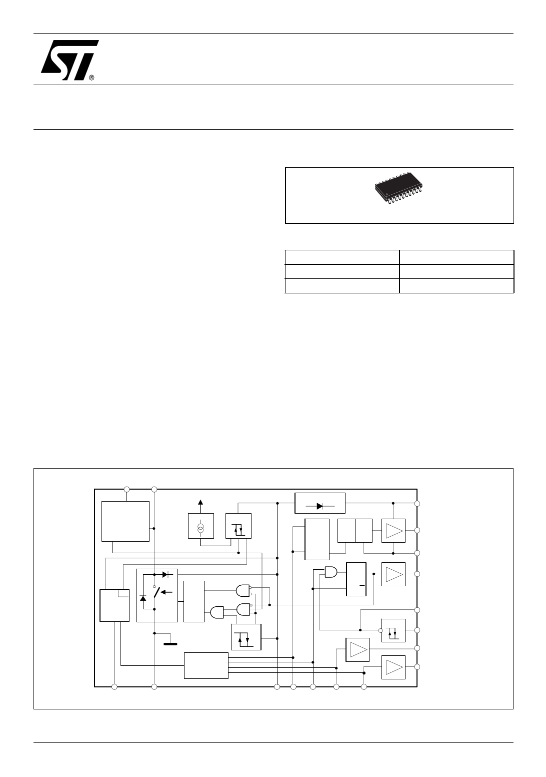
Figure 2. Block Diagram
HVSU
TPR
>600VHIGH
“OVNO” LTAGE
START-UP
G“OEFNF”ERATOR
IC BIAS
µP UVLO
ON
5V
SUPPLY
L
PSW
O
G
I
C
DIM
TPR
BOOTSTRAP
RQ
LEVEL SHIFT
5V 600V
SQ
RQ
SQ
HED
HSD
LSD
OCP
PFD
BOOT
HSG
OUT
LSG
CSO
CSI
HEG
PFG
REF
GND
Vcc HSI LSI HEI PFI
January 2005
Rev. 1
1/14
1 page 
L6382D5
Table 5. Electrical Characteristcs (Tj = 25°C, VCC=12V unless otherwise specified)
Symbol Pin
Parameter
Test condition
min. typ max UNIT
SUPPLY VOLTAGE
VccON
10 Turn-on voltage
13 14 15
V
VccOFF
10 Turn-off voltage
9.3 V
VccSM
10 Save mode voltage
12.75 13.8 14.85 V
VSMhys 10 Save mode hysteresys
0.115
V
VREF(OFF) 10 Reference turn-off
7.65 V
IvccON
10 Start-up current
150 µA
IvccSM
10 Save Mode current
consumption
(1)
190
150 230
µA
µA
Ivcc 10 Quiescent current in Vcc=13V; LGI=HGI=high; no
operating mode
load on VREF.
2 mA
Vz 10 Internal Zener
TBD
V
HIGH VOLTAGE START-UP
IMSS
15 Maximum current
VHVSU > 50V
20
mA
15 Turn-on Voltage
IHVSU=5mA
TBD
V
ILSS
15 Leakage current off state VHVSU = 600V
40 µA
TWO POINT REGULATOR (TPR) PROTECTION
TPRst
10 Vcc Protection level
Operating mode
14.0 15.0 V
TPR(ON)
10 Vcc Turn-on level
Operating mode; after the first 12.5
falling edge on LSG
13.5 V
TPR(OFF) 10 Vcc Turn-off level
Operating mode; after the first 12.45
falling edge on LSG
13.48 V
7 Output voltage on state ITPR = 200mA
2V
7 Forward voltage drop @ 600mA forward current.
Diode
2V
7 Leakage current off state VTPR = 13V
5 µA
LSG, HEG & PFG DRIVERS
VOH(LS) 5, 9, 17 HIGH Output Voltage
ILSG = 10mA
VCC -0.5
V
VOL(LS) 5, 9, 17 LOW Output Voltage
ILSG = 10mA
0.5 V
Sink Current Capability LSG and PFG
120
mA
HEG
50 mA
5/14
5 Page 
L6382D5
external bootstrap diode. This section together with a bootstrap capacitor provides the bootstrap voltage
to drive the high side power MOSFET. This function is achieved using a high voltage DMOS driver
which is driven synchronously with the low side external power MOSFET. For a safe operation, current
flow between BOOT pin and Vcc is always inhibited, even though ZVS operation may not be ensured.
5.4 INTERNAL LOGIC, OVER CURRENT PROTECTION (OCP) AND INTERLOCKING FUNCTION.
The DIM (Digital Input Monitor) block manages the input signals delivered to the drivers ensuring that they
are low during the described start-up procedure; the DIM block controls the L6382D5 behaviour during
both save and operating modes.
When the voltage on pin CSI overcomes the internal reference of 0.54V (typ.) the block latches the fault
condition: in this state the OCP block forces low both HSD and LSD signals while CSO will be forced high.
This condition remains latched until LSI and HSI are simultaneously low and CSI is below 0.54V.
This function is suitable to implement an over current protection or hard-switching detection by using an
external sense resistor.
As the voltage on pin CSI can go negative, the current must be limited below 2mA by external compo-
nents.
Another feature of the DIM block is the internal interlocking that avoids cross-conduction in the half-
bridge FET's: if by chance both HGI and LGI input's are brought high at the same time, then LSG and HSG
are forced low as long as this critical condition persists.
11/14
11 Page | ||
| Páginas | Total 14 Páginas | |
| PDF Descargar | [ Datasheet L6382D5.PDF ] | |
Hoja de datos destacado
| Número de pieza | Descripción | Fabricantes |
| L6382D | Power management unit | ST Microelectronics |
| L6382D5 | POWER MANAGEMENT UNIT FOR MICROCONTROLLED BALLAST | STMicroelectronics |
| L6382D5TR | POWER MANAGEMENT UNIT FOR MICROCONTROLLED BALLAST | STMicroelectronics |
| Número de pieza | Descripción | Fabricantes |
| SLA6805M | High Voltage 3 phase Motor Driver IC. |
Sanken |
| SDC1742 | 12- and 14-Bit Hybrid Synchro / Resolver-to-Digital Converters. |
Analog Devices |
|
DataSheet.es es una pagina web que funciona como un repositorio de manuales o hoja de datos de muchos de los productos más populares, |
| DataSheet.es | 2020 | Privacy Policy | Contacto | Buscar |