|
|
|
PDF VMMK-3503 Data sheet ( Hoja de datos )
| Número de pieza | VMMK-3503 | |
| Descripción | 0.5 - 18 GHz Variable Gain Amplifier | |
| Fabricantes | AVAGO | |
| Logotipo | ||
Hay una vista previa y un enlace de descarga de VMMK-3503 (archivo pdf) en la parte inferior de esta página. Total 12 Páginas | ||
|
No Preview Available !
VMMK-3503
0.5 - 18 GHz Variable Gain Amplifier in SMT Package
Data Sheet
Description
The VMMK-3503 is a small and easy-to-use, broadband,
variable gain amplifier operating in various frequency
bands from 0.5-18 GHz. It is housed in the Avago Tech-
nologies’ industry-leading and revolutionary sub-min-
iature chip scale package (GaAsCap wafer scale leadless
package) which is small and ultra thin yet can be handled
and placed with standard 0402 pick and place assembly
equipment. The VMMK-3503 provides maximum gain of
12 dB with a typical gain range of 23 dB where the gain
control is accessed from the input port by way of a large
value external resistor. It can be operated from 3 V to 5 V
power supply. It is fabricated using Avago Technologies
unique 0.25 μm E-mode PHEMT technology which elimi-
nates the need for negative gate biasing voltage.
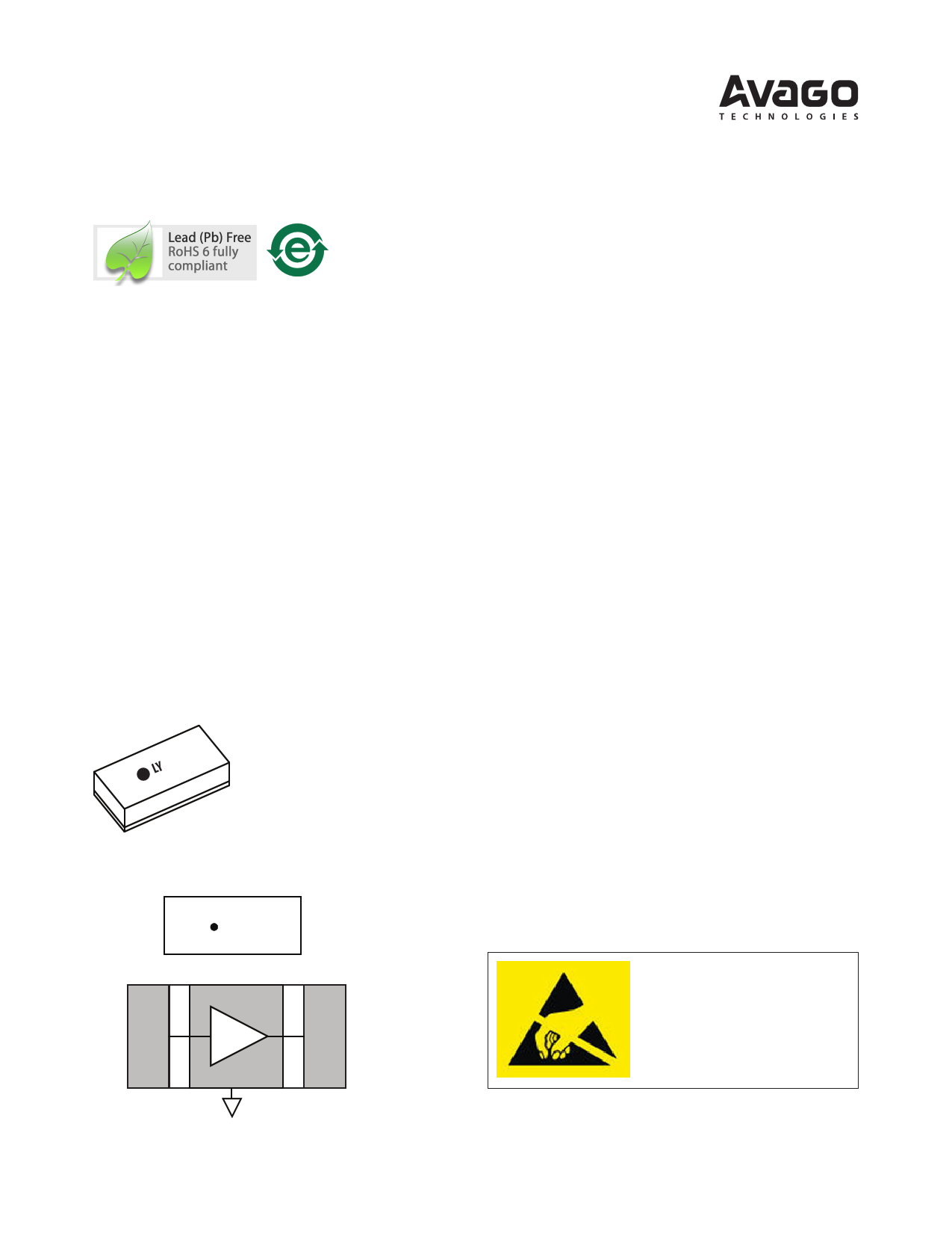
WLP0402, 1 mm x 0.5 mm x 0.25 mm
LY
Features
• 1 x 0.5 mm surface mount package
• Ultrathin (0.25 mm)
• Broadband frequency range: 0.5 to 18 GHz
• In and output match: 50 ohm
• All Positive DC Voltage Supply and Control
• CMOS-compatible gain control voltage
Specifications (6 GHz, Vdd = 5 V, Zin = Zout = 50 Ω)
• Small signal gain: 12 dB typ
• Gain control range: 23 dB typ
• Noise Figure = 3.5 dB typ
Applications
• 2.4, 3.5, and 5-6 GHz WLAN and WiMax
• 802.16 & 802.20 BWA systems
• Radar and ECM systems
• UWB
• Generic IF amplifier and VGA
Pin Connections (Top View)
Input LY
Output
Input Amp
Output
Attention: Observe precautions for
handling electrostatic sensitive devices.
ESD Machine Model = 50 V
ESD Human Body Model = 450 V
Refer to Avago Application Note A004R:
Electrostatic Discharge, Damage and Control.
Note:
“L” = Device Code
“Y” = Month Code
1 page 
VMMK-3503 Typical Performance
(TA = 25° C, Vdd = 5 V, Zin = Zout = 50 Ω unless noted)
15
Vc = 1.8 V
Vc = 0.65 V
10
5
0
-5
0 3 6 9 12 15 18
Freq (GHz)
Figure 7. Input IP3 vs. Freq
20
15
10
5
0
-5
0 0.3 0.6 0.9 1.2
Vc (V)
Figure 8. Input IP3 vs. Vc
1 GHz
6 GHz
12 GHz
18 GHz
1.5 1.8
14 15
12
10 1.8 V
0.9 V
8 0.65 V
6
10
1.8 V
5 0.9 V
0.65 V
0
4 -5
2
0 -10
-2 -15
0 3 6 9 12 15 18
-20 -15 -10
-5
0
5
Freq (GHz)
Pin (dBm)
Figure 9. Saturated Power
Figure 10. Gain vs. Pin at 6 GHz
25
20
15
Vc = 0.65 V
10 Vc = 1.8 V
5
60
Vdd = 5 V
50 Vdd = 4 V
Vdd = 3 V
40
30
20
10
0
0 3 6 9 12 15 18
Freq (GHz)
0
0 0.3 0.6 0.9 1.2 1.5 1.8
Vc (V)
Figure 11. Noise Figure at Min and Max Gain
Figure 12. Supply Current over Bias
5
5 Page 
S Parameter Measurements
The S parameters are measured on a 300 mm G-S-G
(ground signal ground) printed circuit board substrate.
Calibration is achieved with a series of through, short
and open substrates from which an accurate set of S pa-
rameters is created. The test board is 0.016 inch thickness
RO4350. Grounding of the device is achieved with a single
plated through hole directly under the device. The effect
of this plated through hole is included in the S parameter
measurements and is difficult to de-embed accurately.
Since the maximum recommended printed circuit board
thickness is nominally 0.020 inch, then the nominal effect
of printed circuit board grounding can be considered to
have already been included the published S parameters.
Package and Assembly Note
For detailed description of the device package, handling
and assembly, please refer to Application Note 5378.
ESD Precautions
Note: These devices are ESD sensitive. The following pre-
cautions are strongly recommended. Ensure that an ESD
approved carrier is used when die are transported from
one destination to another. Personal grounding is to be
worn at all times when handling these devices. For more
detail, refer to Avago Application Note A004R: Electro-
static Discharge Damage and Control.
Ordering Information
Part Number
VMMK-3503-BLKG
VMMK-3503-TR1G
Devices Per
Container
100
5000
Container
Antistatic Bag
7” Reel
Package Dimension Outline
D
E
A
Note:
All dimensions are in mm
Dimensions
Symbol
E
D
A
Min (mm)
0.500
1.004
0.225
Max (mm)
0.585
1.085
0.275
Reel Orientation
REEL
Device Orientation
USER FEED DIRECTION
4 mm
USER
FEED
DIRECTION
CARRIER
TAPE
TOP VIEW
Notes:
“L” = Device Code
“Y” = Month Code
8 mm
END VIEW
11
11 Page | ||
| Páginas | Total 12 Páginas | |
| PDF Descargar | [ Datasheet VMMK-3503.PDF ] | |
Hoja de datos destacado
| Número de pieza | Descripción | Fabricantes |
| VMMK-3503 | 0.5 - 18 GHz Variable Gain Amplifier | AVAGO |
| Número de pieza | Descripción | Fabricantes |
| SLA6805M | High Voltage 3 phase Motor Driver IC. |
Sanken |
| SDC1742 | 12- and 14-Bit Hybrid Synchro / Resolver-to-Digital Converters. |
Analog Devices |
|
DataSheet.es es una pagina web que funciona como un repositorio de manuales o hoja de datos de muchos de los productos más populares, |
| DataSheet.es | 2020 | Privacy Policy | Contacto | Buscar |