|
|
|
PDF NVT210 Data sheet ( Hoja de datos )
| Número de pieza | NVT210 | |
| Descripción | Temperature Monitor | |
| Fabricantes | ON Semiconductor | |
| Logotipo | ||
Hay una vista previa y un enlace de descarga de NVT210 (archivo pdf) en la parte inferior de esta página. Total 20 Páginas | ||
|
No Preview Available !
NVT210
+15C Temperature Monitor
with Series Resistance
Cancellation
The NVT210 is a dual-channel digital thermometer and
undertemperature/overtemperature alarm, intended for use in thermal
management systems. It is register-compatible with the NCT1008 and
NCT72. A feature of the NVT210 is series resistance cancellation,
where up to 1.5 kW (typical) of resistance in series with the temperature
monitoring diode can be automatically cancelled from the temperature
result, allowing noise filtering. The NVT210 has a configurable ALERT
output and an extended, switchable temperature measurement range.
The NVT210 can measure the temperature of a remote thermal diode
accurate to ±1°C and the ambient temperature accurate to ±3°C. The
temperature measurement range defaults to 0°C to +127°C, compatible
with the NCT1008 and NCT72, but it can be switched to a wider
measurement range of −64°C to +191°C.
The NVT210 communicates over a 2-wire serial interface,
compatible with system management bus (SMBus/I2C) standards. The
default SMBus/I2C address of the NVT210 is 0x4C. An NVT210D is
available with an SMBus/I2C address of 0x4D. This is useful if more
than one NVT210 is used on the same SMBus/I2C.
An ALERT output signals when the on-chip or remote temperature is
out of range. The THERM output is a comparator output that allows
on/off control of a cooling fan. The ALERT output can be reconfigured
as a second THERM output, if required.
The NVT210 has been through Automotive Qualification according to
AEC−Q100 Grade 1 standards.
Features
• On-chip and Remote Temperature Sensor
• 0.25°C Resolution/1°C Accuracy on Remote Channel
• 1°C Resolution/1°C Accuracy on Local Channel
• Series Resistance Cancellation Up to 1.5 kW
• Extended, Switchable Temperature Measurement Range
0°C to +127°C (Default) or –64°C to +191°C
• Register-compatible with NCT1008 and NCT72
• 2-wire SMBus/I2C Serial Interface with SMBus Alert Support
• Programmable Over/Undertemperature Limits
• Offset Registers for System Calibration
• Up to Two Overtemperature Fail-safe THERM Outputs
• 8-lead MSOP Package and a 2 × 2 WDFN8 Package
• 240 mA Operating Current, 5 mA Standby Current
• Automotive Qualification According to AEC−Q100, Grade 1
• Pb-Free Packages are Available
Applications
• Automotive
• Embedded Systems
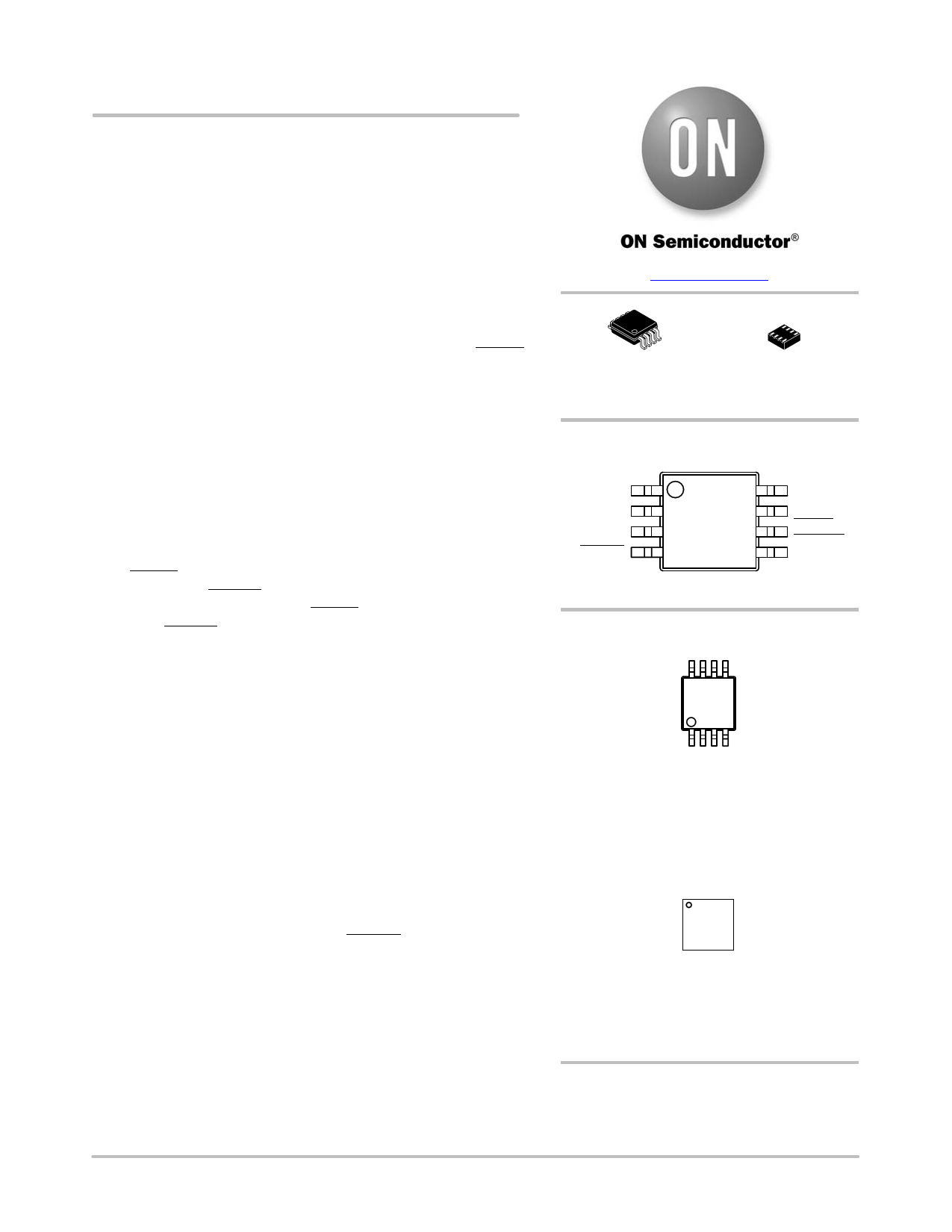
www.onsemi.com
MSOP8
DM SUFFIX
CASE 846A
WDFN8
MT SUFFIX
CASE 511AT
PIN ASSIGNMENT
VDD
D+
D−
THERM
1
SCLK
SDATA
ALERT/
THERM2
GND
(Top View)
MARKING DIAGRAMS
8
XXXX
AYWG
G
1
MSOP8
XXXX
A
Y
W
G
= Specific Device Code
= Assembly Location
= Year
= Work Week
= Pb-Free Package
(Note: Microdot may be in either location)
1
VxMG
G
WDFN8
Vx = Device Code (Where x = C or D)
M = Date Code
G = Pb-Free Package
(Note: Microdot may be in either location)
ORDERING INFORMATION
See detailed ordering and shipping information in the package
dimensions section on page 18 of this data sheet.
© Semiconductor Components Industries, LLC, 2015
May, 2015 − Rev. 8
1
Publication Order Number:
NVT210/D
1 page 
NVT210
TYPICAL PERFORMANCE CHARACTERISTICS
3.5
DEV 1 DEV 8
DEV 15
3.0
DEV 2 DEV 9
DEV 16
DEV 3 DEV 10 MEAN
2.5 DEV 4 DEV 11 HIGH 4R
DEV 5 DEV 12 LOW 4R
2.0
DEV 6
DEV 7
DEV 13
DEV 14
1.5
1.0
0.5
0
−0.5
−1.0
−50
0 50 100
TEMPERATURE (°C)
150
Figure 3. Local Temperature Error vs. Temperature
10
5 D+ To GND
0
−5
−10
D+ To VDD
−15
−20
−25
1
10 100
LEAKAGE RESISTANCE (MW)
Figure 5. Temperature Error vs. D+/D− Leakage
Resistance
3.5
DEV 1 DEV 8
DEV 15
3.0
DEV 2 DEV 9
DEV 16
DEV 3 DEV 10 HIGH 4R
2.5 DEV 4 DEV 11 LOW 4R
DEV 5 DEV 12
2.0 DEV 6 DEV 13
DEV 7 DEV 14
1.5
1.0
0.5
0
−0.5
−1.0
−50
0 50 100
TEMPERATURE (°C)
150
Figure 4. Remote Temperature Error vs. Actual
Temperature
0
−2
−4
−6
−8
−10
DEV 3
−12 DEV 2
−14
DEV 4
−16
−18
0
5 10 15 20
CAPACITANCE (nF)
25
Figure 6. Temperature Error vs. D+/D− Capacitance
1000
900
DEV 2BC
800
700
600
500
DEV 4BC
400
300 DEV 3BC
200
100
0
0.01
0.1 1 10
CONVERSION RATE (Hz)
Figure 7. Operating Supply Current vs.
Conversion Rate
100
422
420
DEV 2BC
418
416
414 DEV 3BC
DEV 4BC
412
410
408
3.0 3.1 3.2 3.3 3.4 3.5 3.6
VDD (V)
Figure 8. Operating Supply Current vs. Voltage
www.onsemi.com
5
5 Page 
NVT210
corresponding value register contains an in-limit
measurement or if the sensor is good.
The ALERT interrupt latch is not reset by reading the
status register. It resets when the ALERT output has been
serviced by the master reading the device address, provided
the error condition has gone away and the status register flag
bits are reset.
When Flag 1 and/or Flag 0 are set, the THERM output
goes low to indicate that the temperature measurements are
outside the programmed limits. The THERM output does
not need to be reset, unlike the ALERT output. Once the
measurements are within the limits, the corresponding status
register bits are automatically reset and the THERM output
goes high. The user may add hysteresis by programming
Register 0x21. The THERM output is reset only when the
temperature falls to limit value minus the hysteresis value.
When Pin 6 is configured as THERM2, only the high
temperature limits are relevant. If Flag 6 and/or Flag 4 are
set, the THERM2 output goes low to indicate that the
temperature measurements are outside the programmed
limits. Flag 5 and Flag 3 have no effect on THERM2. The
behavior of THERM2 is otherwise the same as THERM.
Table 10. STATUS REGISTER BIT ASSIGNMENTS
Bit Name
Function
7
BUSY
1 when ADC is Converting
6 LHIGH 1 when Local High Temperature Limit is
(Note 1) Tripped
5
LLOW
1 when Local Low Temperature Limit is
(Note 1) Tripped
4 RHIGH 1 when Remote High Temperature Limit
(Note 1) is Tripped
3 RLOW 1 when Remote Low Temperature Limit
(Note 1) is Tripped
2
OPEN
1 when Remote Sensor is an Open
(Note 1) Circuit
1 RTHRM 1 when Remote THERM Limit is Tripped
0 LTHRM 1 when Local THERM Limit is Tripped
1. These flags stay high until the status register is read or they are
reset by POR unless Pin 6 is configured as THERM2. Then, only
Bit 2 remains high until the status register is read or is reset by
POR.
Offset Register
Offset errors can be introduced into the remote
temperature measurement by clock noise or when the
thermal diode is located away from the hot spot. To achieve
the specified accuracy on this channel, these offsets must be
removed.
The offset value is stored as a 10-bit, twos complement
value in Register 0x11 (high byte) and Register 0x12 (low
byte, left justified). Only the upper two bits of Register 0x12
are used. The MSB of Register 0x11 is the sign bit. The
minimum, programmable offset is −128°C, and the
maximum is +127.75°C. The value in the offset register is
added to, or subtracted from, the measured value of the
remote temperature.
The offset register powers up with a default value of 0°C
and has no effect unless the user writes a different value to
it.
Table 11. SAMPLE OFFSET REGISTER CODES
Offset Value
−128°C
−4°C
−1°C
−0.25°C
0°C
+0.25°C
+1°C
+4°C
+127.75°C
0x11
1000 0000
1111 1100
1111 1111
1111 1111
0000 0000
0000 0000
0000 0001
0000 0100
0111 1111
0x12
00 00 0000
00 00 0000
00 000000
10 00 0000
00 00 0000
01 00 0000
00 00 0000
00 00 0000
11 00 0000
One-shot Register
The one-shot register is used to initiate a conversion and
comparison cycle when the NVT210 is in standby mode,
after which the device returns to standby. Writing to the
one-shot register address (0x0F) causes the NVT210 to
perform a conversion and comparison on both the internal
and the external temperature channels. This is not a data
register as such, and it is the write operation to Address 0x0F
that causes the one-shot conversion. The data written to this
address is irrelevant and is not stored.
Consecutive ALERT Register
The value written to this register determines how many
out-of-limit measurements must occur before an ALERT is
generated. The default value is that one out-of-limit
measurement generates an ALERT. The maximum value
that can be chosen is 4. The purpose of this register is to
allow the user to perform some filtering of the output. This
is particularly useful at the fastest three conversion rates,
where no averaging takes place. This register is at
Address 0x22.
Table 12. CONSECUTIVE ALERT REGISTER CODES
Register Value
yxxx 000x
Number of Out-of-limit
Measurements Required
1
NOTE:
yxxx 001x
2
yxxx 011x
3
yxxx 111x
4
x = don’t care bits, and y = SMBus timeout bit.
Default = 0. See SMBus section for more information.
www.onsemi.com
11
11 Page | ||
| Páginas | Total 20 Páginas | |
| PDF Descargar | [ Datasheet NVT210.PDF ] | |
Hoja de datos destacado
| Número de pieza | Descripción | Fabricantes |
| NVT210 | Temperature Monitor | ON Semiconductor |
| NVT211 | Temperature Monitor | ON Semiconductor |
| Número de pieza | Descripción | Fabricantes |
| SLA6805M | High Voltage 3 phase Motor Driver IC. |
Sanken |
| SDC1742 | 12- and 14-Bit Hybrid Synchro / Resolver-to-Digital Converters. |
Analog Devices |
|
DataSheet.es es una pagina web que funciona como un repositorio de manuales o hoja de datos de muchos de los productos más populares, |
| DataSheet.es | 2020 | Privacy Policy | Contacto | Buscar |