|
|
|
PDF HC5517 Data sheet ( Hoja de datos )
| Número de pieza | HC5517 | |
| Descripción | 3 REN Ringing SLIC For ISDN Modem/TA and WLL | |
| Fabricantes | Intersil Corporation | |
| Logotipo | ||
Hay una vista previa y un enlace de descarga de HC5517 (archivo pdf) en la parte inferior de esta página. Total 18 Páginas | ||
|
No Preview Available !
Data Sheet
HC5517
July 1998 File Number 4147.2
3 REN Ringing SLIC For ISDN Modem/TA
and WLL
he HC5517 is a ringing SLIC designed to accommodate a wide
variety of local loop applications. The various applications
include, basic POTS lines with answering machines and fax
capabilities, ISDN networks, wireless local loop, and hybrid
fiber coax (HFC) terminals. The HC5517 provides a high
degree of flexibility with open circuit tip to ring DC voltages, user
defined ringing waveforms (sinusoidal to square wave), ring trip
detection thresholds and loop current limits that can be tailored
for many applications. Additional features of the HC5517 are
complex impedance matching, pulse metering and transhybrid
balance. The HC5517 is designed for use in systems where a
separate ring generator is not economically feasible.
The device is manufactured in a high voltage Dielectric Isolation
(DI) process with an operating voltage range from -16V, for off-
hook operation and -80V for ring signal injection. The DI
process provides substrate latch up immunity, resulting in a
robust system design. Together with a secondary protection
diode bridge and “feed” resistors, the device will withstand
1000V lightning induced surges, in a plastic package.
A thermal shutdown with an alarm output and line fault
protection are also included for operation in harsh
environments.
Ordering Information
PART
NUMBER
HC5517IM
HC5517CM
HC5517IB
HC5517CB
TEMP. RANGE
(oC) PACKAGE
-40 to 85 28 Ld PLCC
0 to 75 28 Ld PLCC
-40 to 85 28 SOIC
0 to 75 28 SOIC
PKG. NO.
N28.45
N28.45
M28.3
M28.3
Features
• Thru-SLIC Open Circuit Ringing Voltage up to
77VPEAK/54VRMS, 3 REN Capability at 44VRMS
• Sinusoidal Ringing Capability
• DI Process Provides Substrate Latch Up Immunity when
Driving Inductive Ringers
• Adjustable On-Hook Voltage for Fax and Answering
Machine Compatibility
• Resistive and Complex Impedance Matching
• Programmable Loop Current Limit
• Switch Hook and Adjustable Ring Trip Detection
• Pulse Metering Capability
• Single Low Voltage Positive Supply (+5V)
Applications
• Solid State Line Interface Circuit for Wireless Local Loop,
Hybrid Fiber Coax, Set Top Box, Voice/Data Modems
• Related Literature
- AN9606, Operation of the HC5517 Evaluation Board
- AN9607, Impedance Matching Design Equations
- AN9628, AC Voltage Gain
- AN9608, Implementing Pulse Metering
- AN9636, Implementing an Analog Port for ISDN Using
the HC5517
- AN549, The HC-5502S/4X Telephone Subscriber Line
Interface Circuits (SLIC)
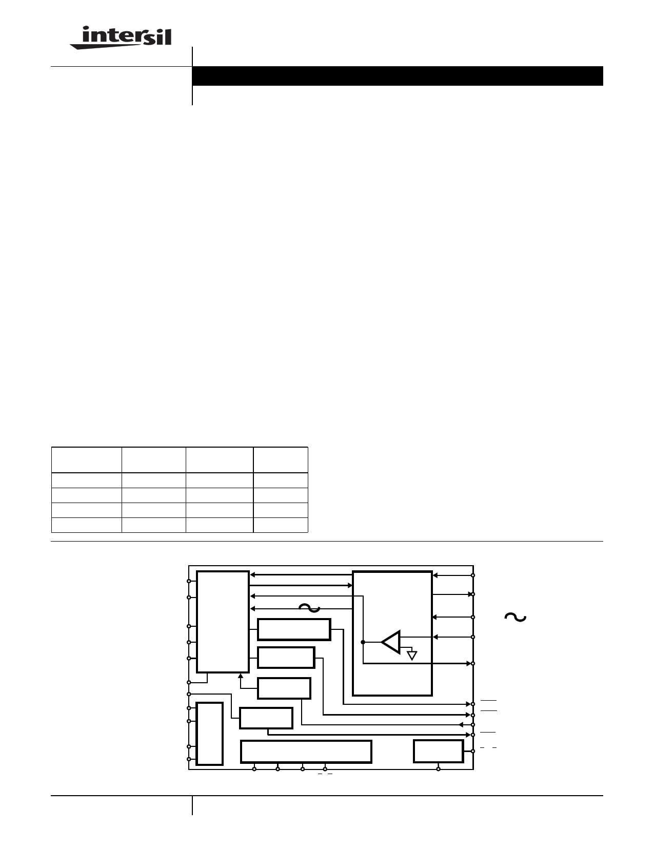
Block Diagram
TIP FEED
TIP SENSE
RING FEED
RING SENSE 1
RING SENSE 2
VREF
RTI
VBAT
VCC
AGND
BGND
2-WIRE
INTERFACE
LOOP CURRENT
DETECTOR
FAULT
DETECTOR
BIAS
CURRENT
LIMIT
RING TRIP
DETECTOR
IIL LOGIC INTERFACE
F1 F0 RS TST
4-WIRE
INTERFACE
+-
RELAY
DRIVER
RDI
VRX
VTX
VRING
- IN 1
OUT 1
SHD
ALM
ILMT
RTD
RDO
60 CAUTION: These devices are sensitive to electrostatic discharge; follow proper IC Handling Procedures.
http://www.intersil.com or 407-727-9207 | Copyright © Intersil Corporation 1999
1 page 
HC5517
Functional Diagram
PLCC / SOIC
R
TF
25
TF
+-
TIP
SENSE
14
R
R
R
R
4.5K
R
R
R/2
R/20
2R
VRX
17
OUT 1
12
+2V
-IN 1
13
VRING
24
+- OP AMP
TA
+-
2R
SHD
15
RING
SENSE 1
RING 16
SENSE 2
100K
100K
100K
100K
4.5K
25K
RA
+-
25K
90K
90K
RTD
FAULT
DET
RF 26
RF
+-
90K VB/2
REF
GM
+-
R = 108kΩ
3
VREF
18
NU
28
RTI
VTX
19
VCC
AGND
21
22
BGND
BIAS
NETWORK
27 VBAT
THERM
LTD
SH
TSD
4
F1
5
F0
6
RS
9
TST
GK
RFC
RF2
11
ILMT
20
RDI
7
SHD
8
RTD
10
ALM
21
RDO
HC5517 TRUTH TABLE
F1 F0
ACTION
0 0 Loop power Denial Active
0 1 Power Down Latch RESET
0 1 Power on RESET
1 0 RD Active
1 1 Normal Loop feed
Over Voltage Protection and Longitudinal Current
Protection
The SLIC device, in conjunction with an external protection
bridge, will withstand high voltage lightning surges and
power line crosses.
High voltage surge conditions are as specified in Table 1.
The SLIC will withstand longitudinal currents up to a
maximum or 30mARMS, 15mARMS per leg, without any
performance degradation
.
PARAMETER
Longitudinal
Surge
Metallic Surge
T/GND
R/GND
50/60Hz Current
T/GND
R/GND
TABLE 1.
TEST
PERFORMANCE
CONDITION
(MAX)
10µs Rise/
1000µs Fall
±1000 (Plastic)
10µs Rise/
1000µs Fall
±1000 (Plastic)
10µs Rise/
1000µs Fall
±1000 (Plastic)
11 Cycles
Limited to
10ARMS
700 (Plastic)
UNITS
VPEAK
VPEAK
PEAK
VRMS
64
5 Page 
HC5517
the SLIC. The signals are Battery Switch, F1 and Ring
Cadence (RC). The active application circuit and active
supervisory function are different for each mode, as shown
in the Table 2.
Mode Control Signals
The Battery Switch selects between the -80V and -24V
supplies. The Battery Switch circuitry is described in the
“Operation of the Battery Switch” section. A system alterna-
tive to the battery switch signal is to use a buffered version of
the SHD output to select the battery voltage. Another alter-
native is to control the output of a programmable battery
supply, removing the battery switch entirely from the applica-
tion circuit. F1 is used to put the SLIC in the power denial
mode. RC drives the base of T2, which is the transistor used
to control the centering voltage and MTU voltage. The three
control signals can be driven from a TTL logic source or an
open collector output
RINGING MODE
The ringing state, as the name indicates, is used to ring the
telephone with a -80V battery supply. The SLIC is designed
for balanced ringing with a differential gain of 40V/V across tip
and ring. Voltage feed amplifiers operating in the linear mode
are used to amplify the ringing signal. The linear amplifier
approach allows the system designer to define the shape and
amplitude of the ringing waveform. Both supervisory function
outputs, SHD and RTD, are active during ringing.
Spectral Content of the Ringing Signal
The shape of the waveform can range from sinusoidal to
trapezoidal. Sinusoidal waveforms are spectrally cleaner
than trapezoidal waveforms, although the latter does result
in lower power dissipation across the SLIC for a given RMS
amplitude. Systems where the ringing signal will be in prox-
imity to digital data lines will benefit from the sinusoidal ring-
ing capability of the HC5517. The slow edge rates of a
sinusoid will minimize coupling of the large amplitude ringing
signal. The linear amplifier architecture of the HC5517
allows the system designer to optimize the design for power
dissipation and spectral purity.
Amplitude of the Ringing Signal
Amplitude control is another benefit of the linear amplifier
architecture. Systems that require less ringing amplitude are
able to do so by driving the HC5517 with a lower level ringing
waveform. Solutions that use saturated amplifiers can only
vary the amplitude of the ringing signal by changing the
negative battery voltage to the SLIC.
HC5517 Through SLIC Ringing
The HC5517 is designed with a high gain input, VRING, that
the system drives while ringing the phone. VRING is one of
many signals summed at the inverting input to the tip feed
amplifier. The gain of the VRING signal through the tip feed
amplifier is set to 20V/V. The output of the tip feed amplifier
is summed at the inverting input of the ring feed amplifier,
configured for unity gain. The result is a differential gain of
40V/V across tip and ring of the ringing signal.
The ringing function requires an input ringing waveform and
a centering voltage. The ringing waveform is the signal from
the 4-wire side that is amplified by the SLIC to ring the tele-
phone. The centering voltage, as previously discussed, is a
positive DC offset that is applied to the VRING input along
with the ringing waveform. The HC5517 application circuit
provides the centering voltage, simplifying the system
interface to an AC coupled ringing waveform.
Ringer Equivalence Number
Before any further discussion, the Ringer Equivalence
Number or REN must be discussed. Based on FCC Part
68.313 a single REN can be defined as 5kΩ, 7kΩ or 8kΩ of
AC impedance at the ringing frequency. The ringing fre-
quency is based on the ringing types listed in Table 1 of the
FCC specification. The impedance of multiple REN is the
paralleling of a single REN. Therefore 5 REN can either be
1kΩ, 1.4kΩ or 1.6kΩ. The 7kΩ model of a single REN will be
used throughout the remainder of the data sheet.
Ringing Waveform
An amplitude of 1.2VRMS will deliver approximately 46VRMS
to a 1 REN load, and 42VRMS to a 3 REN load. The ampli-
tude is REN dependent and is slightly attenuated by the
feedback scheme used for impedance matching. The ringing
waveform is cadenced, alternating between a 20Hz burst
and a silent portion between bursts. Bellcore specification
TR-NWT-000057 defines seven distinct ringing waveforms or
alerting (ringing) patterns. The following table lists each type.
TABLE 1. DISTINCTIVE ALERTING PATTERNS
INTERVAL DURATION IN SECONDS
PATTERN RINGING SILENT RINGING SILENT RINGING SILENT
A 0.4 0.2 0.4 0.2 0.8 4.0
B 0.2 0.1 0.2 0.1 0.6 4.0
C 0.8 0.4 0.8 0.4
D 0.4 0.2 0.6 4.0
E 1.2 4.0
F 1 ± 0.2 3 ± 0.3
G 0.3 0.2 1.0 0.2 0.3 4.0
Figure 8 shows the relationship of the cadenced ringing
waveform and the Battery Switch and RC control signals.
Also shown are the states of the MTU voltage and the
centering voltage.
The state of Battery Switch is indicated by the desired
battery voltage to the SLIC. The RC signal is used to enable
and disable the centering voltage and MTU voltage. RC
follows the ring signal in that it is high during the 20Hz burst
and low during the static part of the waveform.
Open Circuit Voltage During the Ringing Mode
The mutually exclusive relationship of the centering voltage
and MTU implies that both functions will not exist at the
same time. During the silent portion of the ringing waveform
70
11 Page | ||
| Páginas | Total 18 Páginas | |
| PDF Descargar | [ Datasheet HC5517.PDF ] | |
Hoja de datos destacado
| Número de pieza | Descripción | Fabricantes |
| HC55120 | Low Power Universal SLIC Family | Intersil Corporation |
| HC55121 | Low Power Universal SLIC Family | Intersil Corporation |
| HC5513 | TR909 DLC/FLC SLIC with Low Power Standby | Intersil Corporation |
| HC55130 | Low Power Universal SLIC Family | Intersil Corporation |
| Número de pieza | Descripción | Fabricantes |
| SLA6805M | High Voltage 3 phase Motor Driver IC. |
Sanken |
| SDC1742 | 12- and 14-Bit Hybrid Synchro / Resolver-to-Digital Converters. |
Analog Devices |
|
DataSheet.es es una pagina web que funciona como un repositorio de manuales o hoja de datos de muchos de los productos más populares, |
| DataSheet.es | 2020 | Privacy Policy | Contacto | Buscar |