|
|
|
PDF HC5513 Data sheet ( Hoja de datos )
| Número de pieza | HC5513 | |
| Descripción | TR909 DLC/FLC SLIC with Low Power Standby | |
| Fabricantes | Intersil Corporation | |
| Logotipo | ||
Hay una vista previa y un enlace de descarga de HC5513 (archivo pdf) en la parte inferior de esta página. Total 18 Páginas | ||
|
No Preview Available !
Data Sheet
HC5513
October 1998 File Number 3963.10
TR909 DLC/FLC SLIC with
Low Power Standby
The HC5513 is a subscriber line interface circuit which is
interchangeable with Ericsson’s PBL3764 for distributed
central office applications. Enhancements include immunity
to circuit latch-up during hot plug and absence of false
signaling in the presence of longitudinal currents.
The HC5513 is fabricated in a High Voltage Dielectrically
Isolated (DI) Bipolar Process that eliminates leakage
currents and device latch-up problems normally associated
with Junction Isolated (JI) ICs. The elimination of the
leakage currents results in improved circuit performance for
wide temperature extremes. The latch free benefit of the DI
xxprocess guarantees operation under adverse transient
conditions. This process feature makes the HC5513 ideally
suited for use in harsh outdoor environments.
Ordering Information
PART
NUMBER
HC5513BIM
HC5513BIP
TEMP. RANGE
(oC)
PACKAGE
-40 to 85 28 Ld PLCC
-40 to 85 22 Ld PDIP
PKG. NO.
N28.45
E22.4
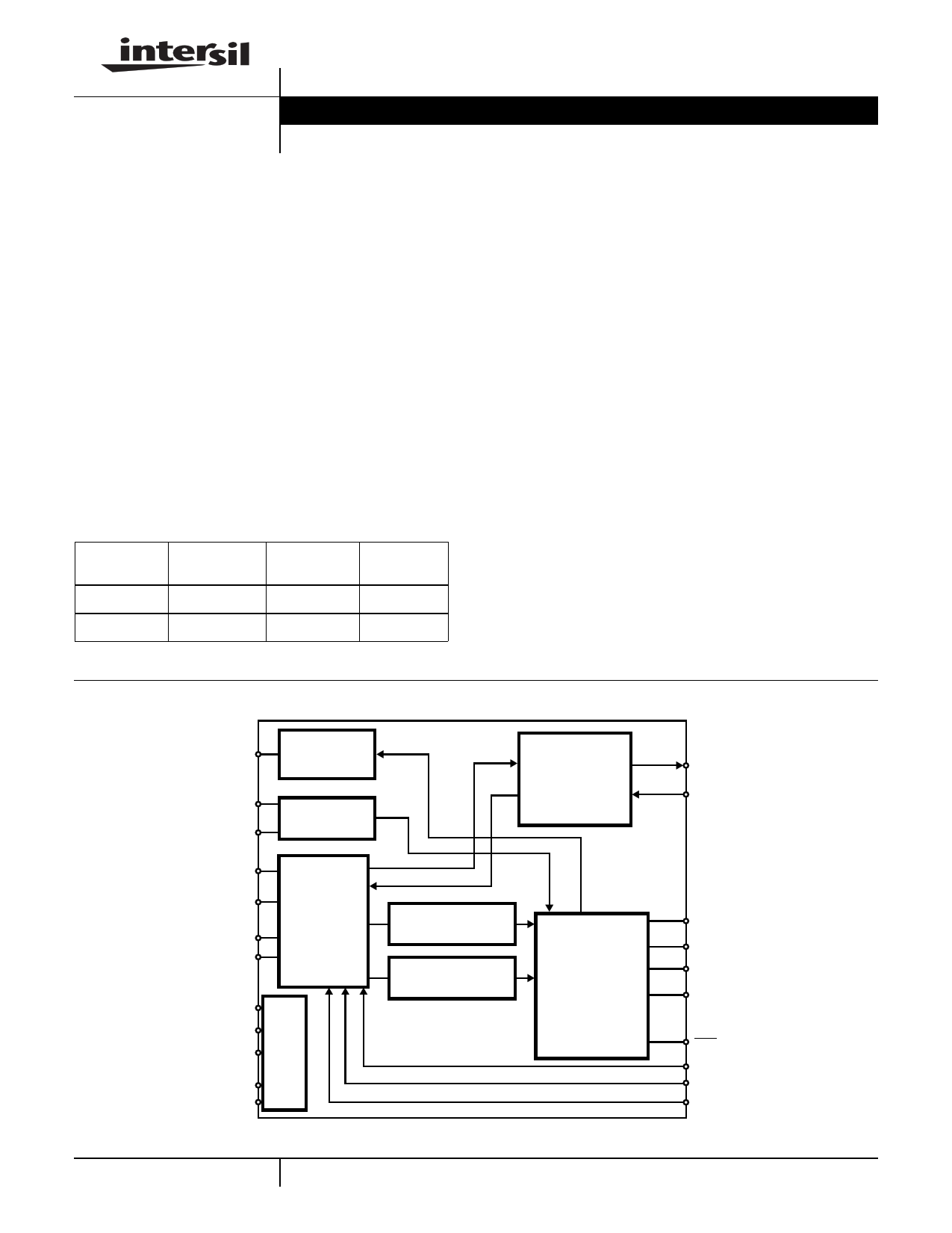
Block Diagram
Features
• DI Monolithic High Voltage Process
• Programmable Current Feed (20mA to 60mA)
• Programmable Loop Current Detector Threshold and Bat-
tery Feed Characteristics
• Ground Key and Ring Trip Detection
• Compatible with Ericsson’s PBL3764
• Thermal Shutdown
• On-Hook Transmission
• Wide Battery Voltage Range (-24V to -58V)
• Low Standby Power
• Meets TR-NWT-000057 Transmission Requirements
• -40oC to 85oC Ambient Temperature Range
Applications
• Digital Loop Carrier Systems . . . . . . . . . . . . . . • Pair Gain
• Fiber-In-The-Loop ONUs . . . . . . . . . . . . . . . . . . . • POTS
• Wireless Local Loop . . . . . . . . . . . . . . . . . . . . . . . .• PABX
• Hybrid Fiber Coax
• Related Literature
- AN9537, Operation of the HC5513/26 Evaluation Board
RINGRLY
DT
DR
TIP
RING
HPT
HPR
RING RELAY
DRIVER
RING TRIP
DETECTOR
2-WIRE
INTERFACE
VBAT
VCC
VEE
AGND
BGND
BIAS
LOOP CURRENT
DETECTOR
GROUND KEY
DETECTOR
4-WIRE
INTERFACE
VF SIGNAL
PATH
DIGITAL
MULTIPLEXER
VTX
RSN
E0
E1
C1
C2
DET
RD
RDC
RSG
54 CAUTION: These devices are sensitive to electrostatic discharge; follow proper IC Handling Procedures.
http://www.intersil.com or 407-727-9207 | Copyright © Intersil Corporation 1999
1 page 
HC5513
Electrical Specifications
TA = -40oC to 85oC, VCC = 5V ±5%, VEE = -5V ±5%, VBAT = -28V, AGND = BGND = 0V, RDC1 = RDC2 =
41.2kΩ, RD = 39kΩ, RSG = ∞, RF1 = RF2 = 0Ω, CHP = 10nF, CDC = 1.5µF, ZL = 600Ω, Unless Otherwise
Specified. All pin number references in the figures refer to the 28 lead PLCC package. (Continued)
PARAMETER
CONDITIONS
MIN
TYP
MAX
UNITS
INSERTION LOSS
2-Wire to 4-Wire
0dBm, 1kHz (Note 19, Figure 9)
-0.2 - 0.2 dB
4-Wire to 2-Wire
0dBm, 1kHz (Note 20, Figure 9)
-0.2 - 0.2 dB
GAIN TRACKING (Ref = -10dBm, at 1.0kHz)
2-Wire to 4-Wire
-40dBm to +3dBm (Note 21, Figure 9)
-0.1 - 0.1 dB
2-Wire to 4-Wire
-55dBm to -40dBm (Note 21, Figure 9)
- ±0.03 -
dB
4-Wire to 2-Wire
-40dBm to +3dBm (Note 22, Figure 9)
-0.1 - 0.1 dB
4-Wire to 2-Wire
-55dBm to -40dBm (Note 22, Figure 9)
- ±0.03 -
dB
GRX = ((VTR1- VTR2)(300k))/(-3)(600)
Where: VTR1 is the Tip to Ring Voltage with VRSN = 0V
and VTR2 is the Tip to Ring Voltage with VRSN = -3V
VRSN = 0V
TIP RSN
27 16
RRX
300kΩ
VRSN = -3V
RL
600Ω
VTR
RDC1
41.2kΩ
RING RDC
28 14
RDC2
41.2kΩ
CDC
1.5µF
C
RL
600Ω
IDCMET
EG
1/ωC << RL
TIP VTX
27 19
VTR
RING RSN
28 16
RT
600kΩ
VTX
RRX
ERX
300kΩ
FIGURE 8. CURRENT GAIN-RSN TO METALLIC
FIGURE 9. FREQUENCY RESPONSE, INSERTION LOSS,
GAIN TRACKING AND HARMONIC DISTORTION
NOISE
Idle Channel Noise at 2-Wire
C-Message Weighting (Note 23,
Figure 10)
- 12 - dBrnC
Idle Channel Noise at 4-Wire
C-Message Weighting (Note 24,
Figure 10)
- 12 - dBrnC
HARMONIC DISTORTION
2-Wire to 4-Wire
0dBm, 1kHz (Note 25, Figure 7)
-
-65 -54
dB
4-Wire to 2-Wire
0dBm, 0.3kHz to 3.4kHz (Note 26,
Figure 9)
-
-65 -54
dB
BATTERY FEED CHARACTERISTICS
Constant Loop Current Tolerance
RDCX = 41.2kΩ
-IL40=o2C5t0o08/(5RoDCC(1N+otReD2C72)),
Loop Current Tolerance (Standby)
I-L40=o(CVBtoAT8-53o)C/(R(NLo+t1e82080)),
Open Circuit Voltage (VTIP - VRING)
-40oC to 85oC, (Active)
0.9IL IL 1.1IL mA
0.8IL IL 1.2IL mA
14 - 20 V
58
5 Page 
HC5513
Transhybrid Circuit
The purpose of the transhybrid circuit is to remove the
receive signal (VRX) from the transmit signal (VTX), thereby
preventing an echo on the transmit side. This is
accomplished by using an external op amp (usually part of
the CODEC) and by the inversion of the signal from the
4-wire receive port (RSN) to the 4-wire transmit port (VTX).
Figure 17 shows the transhybrid circuit. The input signal will
be subtracted from the output signal if I1 equals I2. Node
analysis yields the following equation:
R-V----TT----XX-- + -V--Z--R--B--X-- = 0
(EQ. 21)
The value of ZB is then:
ZB = –RTX • V-V----RT----XX--
Where VRX/VTX equals 1/ A4-4.
Therefore:
ZB = RTX • Z---Z-R---T--X- • -1-------Z0------0--T-----Z-0----L--+---+--2---2R----R-F---F--+-----Z---L--
(EQ. 22)
(EQ. 23)
Example:
Given: RTX = 20kΩ, ZRX = 280kΩ, ZT = 562kΩ (standard
value), RF = 20Ω and ZL= 600Ω,
The value of ZB = 18.7kΩ.
RFB
VTX
RTX
I2
HC5513
ZT
I1
ZB
RSN
ZRX
-
+
+
VTX
-
+
VRX
-
CODEC/
FILTER
FIGURE 17. TRANSHYBRID CIRCUIT
Supervisory Functions
The loop current, ground key and the ring trip detector
outputs are multiplexed to a single logic output pin called
DET. See Table 1 to determine the active detector for a given
logic input. For further discussion of the logic circuitry see
section titled “Digital Logic Inputs”.
Before proceeding with an explanation of the loop current
detector, ground key detector and later the longitudinal
impedance, it is important to understand the difference
between a “metallic” and “longitudinal” loop currents. Figure
18 illustrates 3 different types of loop current encountered.
Case 1 illustrates the metallic loop current. The definition of
a metallic loop current is when equal currents flow out of tip
and into ring. Loop current is a metallic current.
Cases 2 and 3 illustrate the longitudinal loop current. The
definition of a longitudinal loop current is a common mode
current, that flows either out of or into tip and ring
simultaneously. Longitudinal currents in the on-hook state
result in equal currents flowing through the sense resistors
R1 and R2 (Figure 18). And longitudinal currents in the off-
hook state result in unequal currents flowing through the
sense resistors R1 and R2. Notice that for case 2,
longitudinal currents flowing away from the SLIC, the current
through R1 is the metallic loop current plus the longitudinal
current; whereas the current through R2 is the metallic loop
current minus the longitudinal current. Longitudinal currents
are generated when the phone line is influenced by
magnetic fields (e.g., power lines).
Loop Current Detector
Figure 18 shows a simplified schematic of the loop current
and ground key detectors. The loop current detector works
by sensing the metallic current flowing through resistors R1
and R2. This results in a current (IRD) out of the
transconductance amplifier (gm1) that is equal to the product
of gm1 and the metallic loop current. IRD then flows out the
RD pin and through resistor RD to VEE. The value of IRD is
equal to:
IRD = --I--T----I-P-----6–---0--I-0-R----I--N----G---- = 3---I-0-L--0--
(EQ. 24)
The IRD current results in a voltage drop across RD that is
compared to an internal 1.25V reference voltage. When the
voltage drop across RD exceeds 1.25V, and the logic is
configured for loop current detection, the DET pin goes low.
The hysteresis resistor RH adds an additional voltage
effectively across RD, causing the on-hook to off-hook
threshold to be slightly higher than the off-hook to on-hook
threshold.
Taking into account the hysteresis voltage, the typical value
of RD for the on-hook to off-hook condition is:
RD = I--O-----N-----–----H----O-----O----K----4--t-6-o---5--O-----F---F-----–----H----O----O-----K--
(EQ. 25)
Taking into account the hysteresis voltage, the typical value
of RD for the off-hook to on-hook condition is:
RD = I--O-----F----F----–----H----O-----O----K-3---7--t--5o-----O-----N-----–----H----O----O-----K--
(EQ. 26)
64
11 Page | ||
| Páginas | Total 18 Páginas | |
| PDF Descargar | [ Datasheet HC5513.PDF ] | |
Hoja de datos destacado
| Número de pieza | Descripción | Fabricantes |
| HC55120 | Low Power Universal SLIC Family | Intersil Corporation |
| HC55121 | Low Power Universal SLIC Family | Intersil Corporation |
| HC5513 | TR909 DLC/FLC SLIC with Low Power Standby | Intersil Corporation |
| HC55130 | Low Power Universal SLIC Family | Intersil Corporation |
| Número de pieza | Descripción | Fabricantes |
| SLA6805M | High Voltage 3 phase Motor Driver IC. |
Sanken |
| SDC1742 | 12- and 14-Bit Hybrid Synchro / Resolver-to-Digital Converters. |
Analog Devices |
|
DataSheet.es es una pagina web que funciona como un repositorio de manuales o hoja de datos de muchos de los productos más populares, |
| DataSheet.es | 2020 | Privacy Policy | Contacto | Buscar |