|
|
|
PDF FDW2516NZ Data sheet ( Hoja de datos )
| Número de pieza | FDW2516NZ | |
| Descripción | Common Drain N-Channel 2.5V specified PowerTrench MOSFET | |
| Fabricantes | Fairchild Semiconductor | |
| Logotipo | ||
Hay una vista previa y un enlace de descarga de FDW2516NZ (archivo pdf) en la parte inferior de esta página. Total 5 Páginas | ||
|
No Preview Available !
March 2003
FDW2516NZ
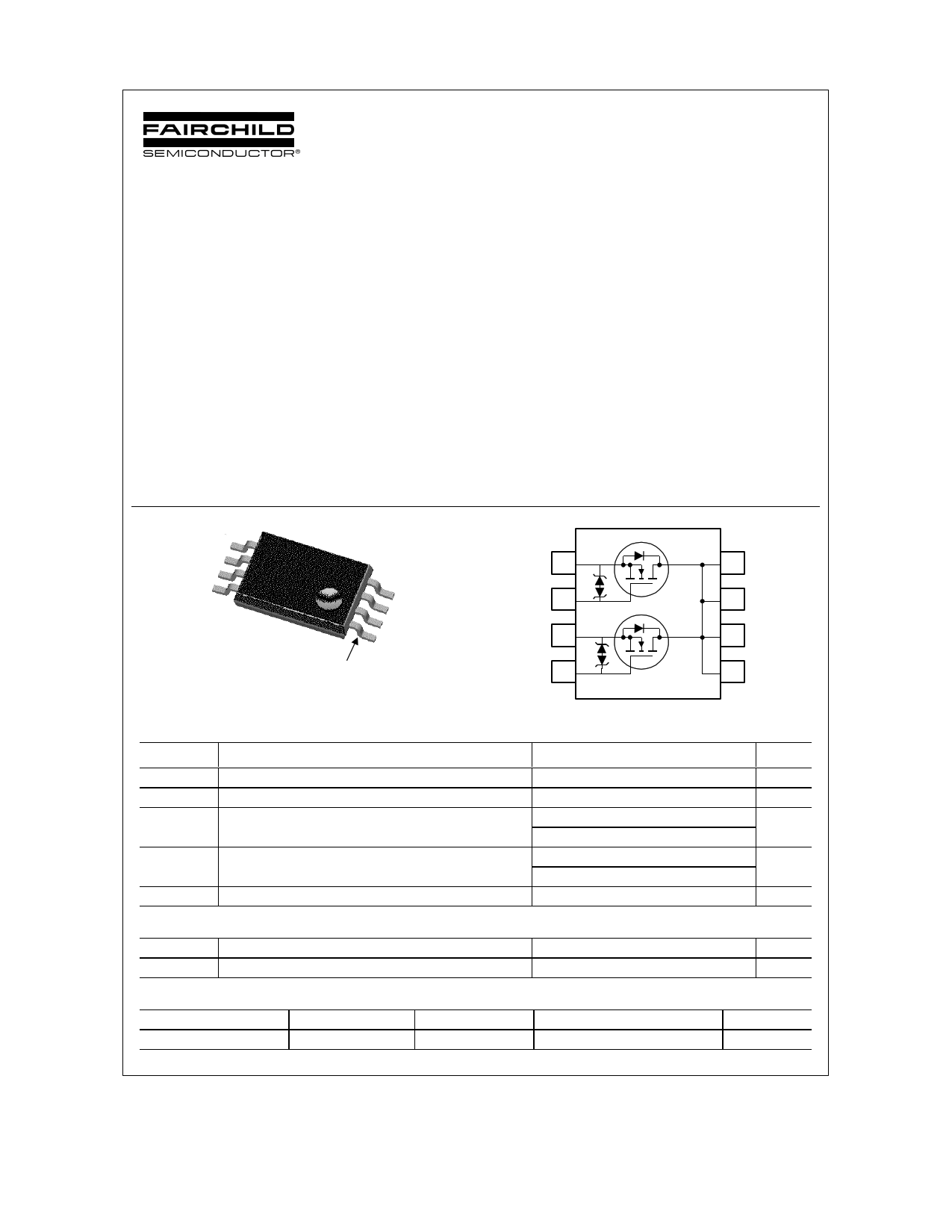
Common Drain N-Channel 2.5V specified PowerTrench® MOSFET
General Description
This dual N-Channel MOSFET has been designed
using Fairchild Semiconductor’s advanced
PowerTrench process to optimize the RDS(ON) @ VGS =
2.5v on special TSSOP-8 lead frame with all the drains
on one side of the package.
Applications
• Li-Ion Battery Pack
Features
• 5.8 A, 20 V
RDS(ON) = 30 mΩ @ VGS = 4.5 V
RDS(ON) = 40 mΩ @ VGS = 2.5 V
• Isolated source and drain pins
• ESD protection diode (note 3)
• High performance trench technology for extremely
low RDS(ON) @ VGS = 2.5 V
• Low profile TSSOP-8 package
D
D
D
D
TSSOP-8
G2
S2
G1
S1
Pin 1
1
2
3
4
8
7
6
5
Absolute Maximum Ratings TA=25oC unless otherwise noted
Symbol
Parameter
VDSS
VGSS
ID
Drain-Source Voltage
Gate-Source Voltage
Drain Current – Continuous
– Pulsed
(Note 1a)
PD
Power Dissipation for Single Operation
(Note 1a)
(Note 1b)
TJ, TSTG
Operating and Storage Junction Temperature Range
Thermal Characteristics
RθJA Thermal Resistance, Junction-to-Ambient
RθJA Thermal Resistance, Junction-to-Ambient
(Note 1a)
(Note 1b)
Package Marking and Ordering Information
Device Marking
Device
Reel Size
2516NZ
FDW2516NZ
13’’
Ratings
20
±12
5.8
20
1.6
1.1
–55 to +150
77
114
Tape width
12mm
Units
V
V
A
W
°C
°C/W
°C/W
Quantity
3000 units
©2003 Fairchild Semiconductor Corporation
FDW2516NZ Rev B
1 page 
Typical Characteristics
10
ID = 5.8A
8
6
4
VDS = 5V
10V
15V
2
0
0 5 10 15 20
Qg, GATE CHARGE (nC)
Figure 7. Gate Charge Characteristics.
100
RDS(ON) LIMIT
10
1
VGS = 4.5V
0.1
SINGLE PULSE
RθJA = 114oC/W
TA = 25oC
100us
1ms
10ms
100ms
1s
10s
DC
0.01
0.1
1 10
VDS, DRAIN-SOURCE VOLTAGE (V)
100
Figure 9. Maximum Safe Operating Area.
1200
900
600
f = 1MHz
VGS = 0 V
Ciss
300
Crss
0
0
Coss
4 8 12 16
VDS, DRAIN TO SOURCE VOLTAGE (V)
20
Figure 8. Capacitance Characteristics.
50
SINGLE PULSE
40 RθJA = 114°C/W
TA = 25°C
30
20
10
0
0.001
0.01
0.1 1
10
t1, TIME (sec)
100 1000
Figure 10. Single Pulse Maximum
Power Dissipation.
1
0.1
0.01
D = 0.5
0.2
0.1
0.05
0.02
0.01
SINGLE PULSE
0.001
0.0001
0.001
0.01
0.1 1
t1, TIME (sec)
RθJA(t) = r(t) * RθJA
RθJA =114 °C/W
P(pk)
t1
t2
TJ - TA = P * RθJA(t)
Duty Cycle, D = t1 / t2
10 100 1000
Figure 11. Transient Thermal Response Curve.
Thermal characterization performed using the conditions described in Note 1b.
Transient thermal response will change depending on the circuit board design.
FDW2516NZ Rev B
5 Page | ||
| Páginas | Total 5 Páginas | |
| PDF Descargar | [ Datasheet FDW2516NZ.PDF ] | |
Hoja de datos destacado
| Número de pieza | Descripción | Fabricantes |
| FDW2516NZ | Common Drain N-Channel 2.5V specified PowerTrench MOSFET | Fairchild Semiconductor |
| Número de pieza | Descripción | Fabricantes |
| SLA6805M | High Voltage 3 phase Motor Driver IC. |
Sanken |
| SDC1742 | 12- and 14-Bit Hybrid Synchro / Resolver-to-Digital Converters. |
Analog Devices |
|
DataSheet.es es una pagina web que funciona como un repositorio de manuales o hoja de datos de muchos de los productos más populares, |
| DataSheet.es | 2020 | Privacy Policy | Contacto | Buscar |