|
|
|
PDF HCPL-3000 Data sheet ( Hoja de datos )
| Número de pieza | HCPL-3000 | |
| Descripción | Power Bipolar Transistor Base Drive Optocoupler | |
| Fabricantes | Agilent(Hewlett-Packard) | |
| Logotipo | ||
Hay una vista previa y un enlace de descarga de HCPL-3000 (archivo pdf) en la parte inferior de esta página. Total 9 Páginas | ||
|
No Preview Available !
Power Bipolar Transistor
Base Drive Optocoupler
Technical Data
H
HCPL-3000
Features
• High Output Current
IO2 (2.0 A Peak, 0.6 A
Continuous)
IO1 (1.0 A Peak, 0.5 A
Continuous)
• 1.5 kV/µs Minimum Common
Mode Rejection (CMR) at
VCM = 600 V
• Wide VCC Range (5.4 to 13
Volts)
• 2 µs Typical Propagation
Delay
• Recognized under UL 1577
for Dielectric Withstand
Proof Test Voltage of 5000
Vac, 1 Minute
Description
The HCPL-3000 consists of a
Silicon-doped GaAs LED optically
coupled to an integrated circuit
with a power output stage. This
optocoupler is suited for driving
power bipolar transistors and
power Darlington devices used in
motor control inverter applica-
tions. The high peak and steady
state current capabilities of the
output stage allow for direct
interfacing to the power device
without the need for an interme-
diate amplifier stage. With a CMR
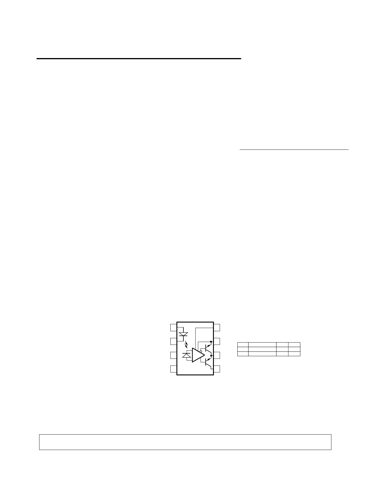
Functional Diagram
rating of 1.5 kV/µs this optocoup-
ler readily rejects transients found
in inverter applications.
The LED controls the state of the
output stage. Transistor Q2 in the
output stage is on with the LED
off, allowing the base of the
power device to be held low.
Turning on the LED turns off
transistor Q2 and switches on
transistor Q1 in the output stage
which provides current to drive
the base of a power bipolar
device.
Applications
• Isolated Bipolar Transistor
Base Drive
• AC and DC Motor Drives
• General Purpose Industrial
Inverters
• Uninterruptable Power
Supply
ANODE 1
CATHODE 2
3
4
HCPL-3000
8 VCC
7 GND
Q2
6 VO2
Q1
5 VO1
TRUTH TABLE
LED OUTPUT
ON HIGH LEVEL
OFF LOW LEVEL
Q1
ON
OFF
Q2
OFF
ON
THE USE OF A 0.1µF BYPASS CAPACITOR CONNECTED BETWEEN PINS 8 AND 7 IS RECOMMENDED. ALSO, CURRENT LIMITING
RESISTORS ARE RECOMMENDED (SEE FIGURE 1, NOTE 2, AND NOTE 7).
CAUTION: It is advised that normal static precautions be taken in handling and assembly of this component to
prevent damage and/or degradation which may be induced by ESD.
5965-3584E
1-329
1 page 
Switching Specifications (TA = 25°C)
Parameter
Sym. Min. Typ. Max. Units
Test Conditions
Fig. Note
Propagation Delay
Time to High Output
Level
tPLH
-
2 5 µs VCC = 6 V, IF = 5 mA,
7, 2, 6
RL1 = 5 Ω, RL2 = 10 Ω
24,
25
Propagation Delay Time tPHL - 2 5
to Low Output Level
Rise Time
Fall Time
Output High Level
Common Mode
Transient Immunity
Output Low Level
Common Mode
Transient Immunity
tr - 0.2 1
tf - 0.1 1
|CMH| 1500 -
- V/µs VCM = 600 V Peak,
8
IF = 5mA, RL1 = 470 Ω,
RL2 = 1 kΩ, ∆V02H = 0.5 V
|CML| 1500 -
- V/µs VCM = 600 V Peak,
IF = 0 mA, RL1 = 470 Ω,
RL2 = 1 kΩ, ∆V02L = 0.5 V
2
Package Characteristics
Parameter
Sym. Min. Typ. Max. Units
Test Conditions
Fig. Note
Input-Output Momentary VISO 5000
Withstand Voltage*
V rms RH = 40% to 60%,
t = 1 min., TA = 25°C
Resistance
(Input-Output)
RI-O 5x10¹⁰ 1011
–
Ω VI-O = 500 V, TA = 25°C,
RH = 40% to 60%
4, 5
4
Capacitance
(Input-Output)
CI-O – 1.2 –
pF f = 1 MHz
4
*The Input-Output Momentary Withstand Voltage is a dielectric voltage rating that should not be interpreted as an input-output
continuous voltage rating. For the continuous voltage rating refer to the VDE 0884 Insulation Characteristics Table (if applicable), your
equipment level safety specification, or HP Application Note 1074, “Optocoupler Input-Output Endurance Voltage.”
Notes:
1. Derate absolute maximum ratings with ambient temperatures as shown in Figures 9, 10, and 11.
2. A bypass capacitor of 0.01 µF or more is needed near the device between VCC and GND when measuring output and transfer
characteristics.
3. IFLH represents the forward current when the output goes from low to high.
4. Device considered a two terminal device; pins 1-4 are shorted together and pin 5-8 are shorted together.
5. For devices with minimum VISO specified at 5000 V rms, in accordance with UL1577, each optocoupler is proof-tested by applying an
insulation test voltage ≥ 6000 Vrms for one second (leakage current detection limit, II-O ≤ 200 µA).
6. The tPLH and tPHL propagation delays are measured from the 50% level of the input pulse to the 50% level of the output pulse.
7. R1 sets the base current (IO1 in Figure 1) supplied to the power bipolar device. R2 limits the peak current seen by Q2 when the device
is turning off. For more applications and circuit design information see Application Note “Power Transistor Gate/Base Drive
Optocouplers.”
1-333
5 Page | ||
| Páginas | Total 9 Páginas | |
| PDF Descargar | [ Datasheet HCPL-3000.PDF ] | |
Hoja de datos destacado
| Número de pieza | Descripción | Fabricantes |
| HCPL-3000 | Power Bipolar Transistor Base Drive Optocoupler | Agilent(Hewlett-Packard) |
| Número de pieza | Descripción | Fabricantes |
| SLA6805M | High Voltage 3 phase Motor Driver IC. |
Sanken |
| SDC1742 | 12- and 14-Bit Hybrid Synchro / Resolver-to-Digital Converters. |
Analog Devices |
|
DataSheet.es es una pagina web que funciona como un repositorio de manuales o hoja de datos de muchos de los productos más populares, |
| DataSheet.es | 2020 | Privacy Policy | Contacto | Buscar |