|
|
|
PDF P5NC50FP Data sheet ( Hoja de datos )
| Número de pieza | P5NC50FP | |
| Descripción | STP5NC50FP | |
| Fabricantes | ST Microelectronics | |
| Logotipo | ||
Hay una vista previa y un enlace de descarga de P5NC50FP (archivo pdf) en la parte inferior de esta página. Total 12 Páginas | ||
|
No Preview Available !
STP5NC50 - STP5NC50FP
STB5NC50 - STB5NC50-1
N-CHANNEL 500V - 1.3Ω - 5.5A TO-220/FP/D2PAK/I2PAK
PowerMesh™ II MOSFET
TYPE
VDSS
RDS(on)
ID
STP5NC50
STP5NC50FP
STB5NC50
STB5NC50-1
500 V
500 V
500 V
500 V
< 1.5Ω
< 1.5Ω
< 1.5Ω
< 1.5Ω
5.5A
5.5A
5.5A
5.5A
s TYPICAL RDS(on) = 1.3Ω
s EXTREMELY HIGH dv/dt CAPABILITY
s 100% AVALANCHE TESTED
s NEW HIGH VOLTAGE BENCHMARK
s GATE CHARGE MINIMIZED
DESCRIPTION
The PowerMESH™ II is the evolution of the first
generation of MESH OVERLAY™ . The layout re-
finements introduced greatly improve the Ron*area
figure of merit while keeping the device at the lead-
ing edge for what concerns swithing speed, gate
charge and ruggedness.
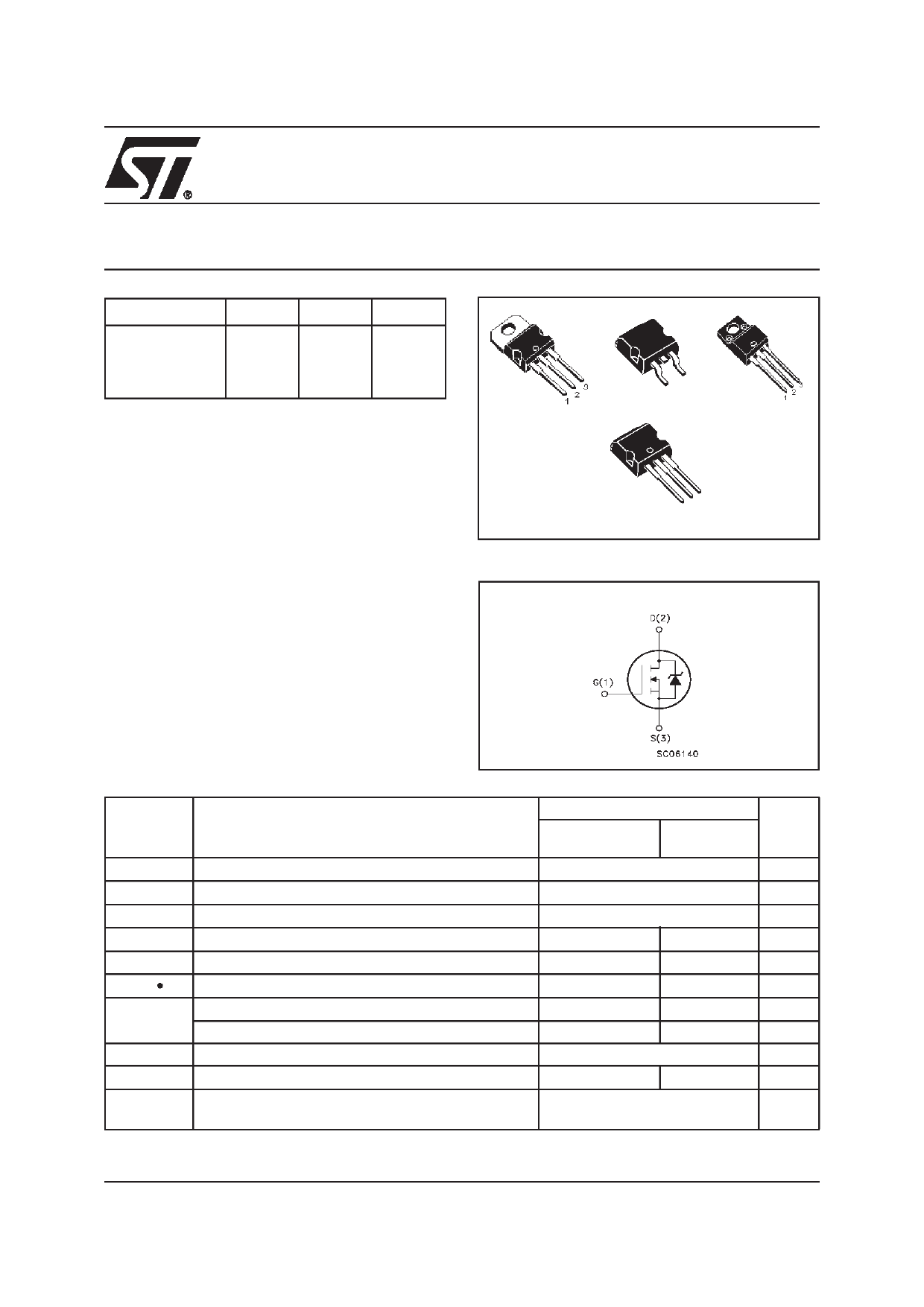
TO-220
3
1
D2PAK
TO-220FP
123
I2PAK
INTERNAL SCHEMATIC DIAGRAM
APPLICATIONS
s HIGH CURRENT, HIGH SPEED SWITCHING
s SWITH MODE POWER SUPPLIES (SMPS)
s DC-AC CONVERTERS FOR WELDING
EQUIPMENT AND UNINTERRUPTIBLE
POWER SUPPLIES AND MOTOR DRIVES
ABSOLUTE MAXIMUM RATINGS
Symbol
Parameter
VDS Drain-source Voltage (VGS = 0)
VDGR
Drain-gate Voltage (RGS = 20 kΩ)
VGS Gate- source Voltage
ID Drain Current (continuos) at TC = 25°C
ID Drain Current (continuos) at TC = 100°C
IDM ( ) Drain Current (pulsed)
PTOT
Total Dissipation at TC = 25°C
Derating Factor
dv/dt(1) Peak Diode Recovery voltage slope
VISO
Insulation Withstand Voltage (DC)
Tj Operating Junction Temperature
Tstg Storage Temperature
(•)Pulse width limited by safe operating area
(1)ISD ≤5.5A, di/dt ≤100A/µs, VDD ≤ V(BR)DSS, Tj ≤ TJMAX.
December 2002
Value
STP5NC50
STB5NC50/-1
STP5NC50FP
500
500
±30
5.5 5.5(*)
3.5 3.5(*)
22 22
100 35
0.8 0.28
3.5
- 2500
-55 to 175
-65 to 175
(*)Limited only by maximum temperature allowed
Unit
V
V
V
A
A
A
W
W/°C
V/ns
V
°C
°C
1/12
1 page 
STP5NC50 - STP5NC50FP - STB5NC50 - STB5NC50-1
Gate Charge vs Gate-source Voltage
Capacitance Variations
Normalized Gate Threshold Voltage vs Temp. Normalized On Resistance vs Temperature
Source-drain Diode Forward Characteristics
5/12
5 Page 
STP5NC50 - STP5NC50FP - STB5NC50 - STB5NC50-1
D2PAK FOOTPRINT
TUBE SHIPMENT (no suffix)*
TAPE AND REEL SHIPMENT (suffix ”T4”)*
TAPE MECHANICAL DATA
DIM.
A0
B0
D
D1
E
F
K0
P0
P1
P2
R
T
W
mm inch
MIN. MAX. MIN. MAX.
10.5 10.7 0.413 0.421
15.7 15.9 0.618 0.626
1.5 1.6 0.059 0.063
1.59 1.61 0.062 0.063
1.65 1.85 0.065 0.073
11.4 11.6 0.449 0.456
4.8 5.0 0.189 0.197
3.9 4.1 0.153 0.161
11.9 12.1 0.468 0.476
1.9 2.1 0.075 0.082
50 1.574
0.25 0.35 0.0098 0.0137
23.7 24.3 0.933 0.956
* on sales type
REEL MECHANICAL DATA
DIM.
A
B
C
D
G
N
T
mm inch
MIN. MAX. MIN. MAX.
330 12.992
1.5 0.059
12.8 13.2 0.504 0.520
20.2 0795
24.4 26.4 0.960 1.039
100 3.937
30.4 1.197
BASE QTY
1000
BULK QTY
1000
11/12
11 Page | ||
| Páginas | Total 12 Páginas | |
| PDF Descargar | [ Datasheet P5NC50FP.PDF ] | |
Hoja de datos destacado
| Número de pieza | Descripción | Fabricantes |
| P5NC50FP | STP5NC50FP | ST Microelectronics |
| Número de pieza | Descripción | Fabricantes |
| SLA6805M | High Voltage 3 phase Motor Driver IC. |
Sanken |
| SDC1742 | 12- and 14-Bit Hybrid Synchro / Resolver-to-Digital Converters. |
Analog Devices |
|
DataSheet.es es una pagina web que funciona como un repositorio de manuales o hoja de datos de muchos de los productos más populares, |
| DataSheet.es | 2020 | Privacy Policy | Contacto | Buscar |