|
|
|
PDF ADSP-21160MKBZ-80 Data sheet ( Hoja de datos )
| Número de pieza | ADSP-21160MKBZ-80 | |
| Descripción | Digital Signal Processor | |
| Fabricantes | Analog Devices | |
| Logotipo | ||
Hay una vista previa y un enlace de descarga de ADSP-21160MKBZ-80 (archivo pdf) en la parte inferior de esta página. Total 30 Páginas | ||
|
No Preview Available !
SUMMARY
High performance 32-bit DSP—applications in audio, medi-
cal, military, graphics, imaging, and communication
Super Harvard architecture—4 independent buses for dual
data fetch, instruction fetch, and nonintrusive, zero-over-
head I/O
Backward compatible—assembly source level compatible
with code for ADSP-2106x DSPs
Single-instruction, multiple-data (SIMD) computational
architecture—two 32-bit IEEE floating-point computation
units, each with a multiplier, ALU, shifter, and register file
Integrated peripherals—integrated I/O processor, 4M bits
on-chip dual-ported SRAM, glueless multiprocessing fea-
tures, and ports (serial, link, external bus, and JTAG)
SHARC
Digital Signal Processor
ADSP-21160M/ADSP-21160N
FEATURES
100 MHz (10 ns) core instruction rate (ADSP-21160N)
Single-cycle instruction execution, including SIMD opera-
tions in both computational units
Dual data address generators (DAGs) with modulo and bit-
reverse addressing
Zero-overhead looping and single-cycle loop setup, provid-
ing efficient program sequencing
IEEE 1149.1 JTAG standard Test Access Port and on-chip
emulation
400-ball 27 mm × 27 mm PBGA package
Available in lead-free (RoHS compliant) package
200 million fixed-point MACs sustained performance
(ADSP-21160N)
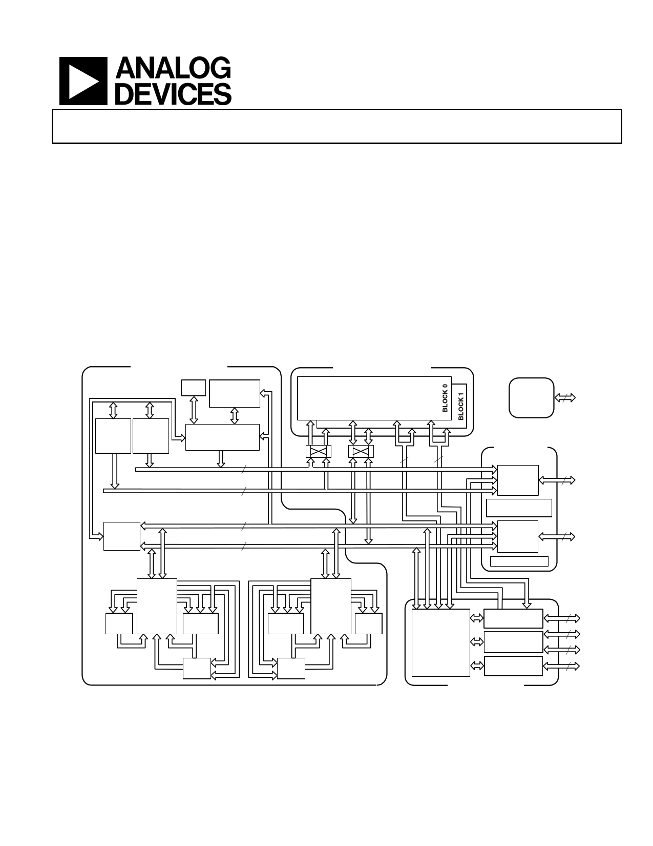
CORE PROCESSOR
TIMER
INSTRUCTION
CACHE
32 x 48-BIT
DAG1
DAG2
8 x 4 x 32 8 x 4 x 32
PROGRAM
SEQUENCER
PM ADDRESS BUS
32
DM ADDRESS BUS
32
BUS
CONNECT
(PX)
PM DATA BUS 16/32/40/48/64
DM DATA BUS
32/40/64
DUAL-PORTED SRAM
TWO INDEPENDENT
DUAL-PORTED BLOCKS
PROCESSOR PORT
I/O PORT
ADDR
DATA
DATA ADDR
ADDR
DATA
DATA ADDR
IOD IOA
64 18
JTAG
TEST AND
EMULATION
6
EXTERNAL
PORT
ADDR BUS
MUX
32
MULTIPROCESSOR
INTERFACE
DATA BUS
MUX
64
HOST PORT
MULT
DATA
REGISTER
FILE
(PEX)
16 x 40-BIT
BARREL
SHIFTER
ALU
BARREL
SHIFTER
DATA
REGISTER
FILE
(PEY)
16 x 40-BIT
MULT
ALU
IOP
REGISTERS
(MEMORY
MAPPED)
CONTROL,
STATUS AND
DATA BUFFERS
DMA
CONTROLLER
SERIAL PORTS
(2)
LINK PORTS
(6)
I/O PROCESSOR
4
6
6
60
Figure 1. Functional Block Diagram
SHARC and the SHARC logo are registered trademarks of Analog Devices, Inc.
Rev. C
Document Feedback
Information furnished by Analog Devices is believed to be accurate and reliable.
However, no responsibility is assumed by Analog Devices for its use, nor for any
infringements of patents or other rights of third parties that may result from its use.
Specifications subject to change without notice. No license is granted by implication
or otherwise under any patent or patent rights of Analog Devices. Trademarks and
registered trademarks are the property of their respective owners.
One Technology Way, P.O. Box 9106, Norwood, MA 02062-9106 U.S.A.
Tel: 781.329.4700
©2013 Analog Devices, Inc. All rights reserved.
Technical Support
www.analog.com
1 page 
CLOCK
4
3
4
LINK
DEVICES
(6 MAX)
(OPTIONAL)
SERIAL
DEVICE
(OPTIONAL)
SERIAL
DEVICE
(OPTIONAL)
ADSP-21160X
CLKIN
BMS
CLK_CFG3–0
EBOOT
CIF
LBOOT
BRST
IRQ2–0
ADDR31–0
FLAG3–0
TIMEXP DATA63–0
LXCLK
LXACK
LXDAT7–0
RDx
WRx
ACK
MS3–0
TCLK0
RCLK0
TFS0
RSF0
DT0
DR0
TCLK1
RCLK1
TFS1
RSF1
DT1
DR1
PAGE
SBTS
CLKOUT
DMAR1–2
DMAG1–2
CS
HBR
HBG
REDY
RPBA
ID2–0
BR1–6
PA
RESET JTAG
6
CS BOOT
ADDR EPROM
(OPTIONAL)
DATA
ADDR
DATA MEMORY/
OE MAPPED
DEVICES
WE (OPTIONAL)
ACK
CS
DMA DEVICE
(OPTIONAL)
DATA
HOST
PROCESSOR
INTERFACE
(OPTIONAL)
ADDR
DATA
Figure 2. Single-Processor System
enabled, the same instruction is executed in both processing ele-
ments, but each processing element operates on different data.
This architecture is efficient at executing math-intensive DSP
algorithms.
Entering SIMD mode also has an effect on the way data is trans-
ferred between memory and the processing elements. In SIMD
mode, twice the data bandwidth is required to sustain computa-
tional operation in the processing elements. Because of this
requirement, entering SIMD mode also doubles the bandwidth
between memory and the processing elements. When using the
DAGs to transfer data in SIMD mode, two data values are trans-
ferred with each access of memory or the register file.
Independent, Parallel Computation Units
Within each processing element is a set of computational units.
The computational units consist of an arithmetic/logic unit
(ALU), multiplier, and shifter. These units perform single-cycle
instructions. The three units within each processing element are
arranged in parallel, maximizing computational throughput.
Single multifunction instructions execute parallel ALU and
multiplier operations. In SIMD mode, the parallel ALU and
multiplier operations occur in both processing elements. These
computation units support IEEE 32-bit single-precision float-
ing-point, 40-bit extended-precision floating-point, and 32-bit
fixed-point data formats.
ADSP-21160M/ADSP-21160N
Data Register File
A general-purpose data register file is contained in each pro-
cessing element. The register files transfer data between the
computation units and the data buses, and store intermediate
results. These 10-port, 32-register (16 primary, 16 secondary)
register files, combined with the ADSP-2116x enhanced
Harvard architecture, allow unconstrained data flow between
computation units and internal memory. The registers in PEX
are referred to as R0–R15 and in PEY as S0–S15.
Single-Cycle Fetch of Instruction and Four Operands
The processor features an enhanced Harvard architecture in
which the data memory (DM) bus transfers data, and the pro-
gram memory (PM) bus transfers both instructions and data
(see the functional block diagram 1). With the ADSP-21160x
DSP’s separate program and data memory buses and on-chip
instruction cache, the processor can simultaneously fetch four
operands and an instruction (from the cache), all in a single
cycle.
Instruction Cache
The ADSP-21160x includes an on-chip instruction cache that
enables three-bus operation for fetching an instruction and four
data values. The cache is selective—only the instructions whose
fetches conflict with PM bus data accesses are cached. This
cache allows full-speed execution of core, providing looped
operations, such as digital filter multiply- accumulates and FFT
butterfly processing.
Data Address Generators with Hardware Circular Buffers
The ADSP-21160x DSP’s two data address generators (DAGs)
are used for indirect addressing and provide for implementing
circular data buffers in hardware. Circular buffers allow efficient
programming of delay lines and other data structures required
in digital signal processing, and are commonly used in digital
filters and Fourier transforms. The two DAGs of the product
contain sufficient registers to allow the creation of up to 32 cir-
cular buffers (16 primary register sets, 16 secondary). The DAGs
automatically handle address pointer wraparound, reducing
overhead, increasing performance, and simplifying implemen-
tation. Circular buffers can start and end at any memory
location.
Flexible Instruction Set
The 48-bit instruction word accommodates a variety of parallel
operations for concise programming. For example, the proces-
sor can conditionally execute a multiply, an add, and subtract,
in both processing elements, while branching, all in a single
instruction.
Rev. C | Page 5 of 60 | February 2013
5 Page 
ADSP-21160M/ADSP-21160N
PIN FUNCTION DESCRIPTIONS
ADSP-21160x pin definitions are listed below. Inputs identified
as synchronous (S) must meet timing requirements with respect
to CLKIN (or with respect to TCK for TMS, TDI). Inputs iden-
tified as asynchronous (A) can be asserted asynchronously to
CLKIN (or to TCK for TRST).
Tie or pull unused inputs to VDD or GND, except for the
following:
• ADDR31–0, DATA63–0, PAGE, BRST, CLKOUT (ID2–0
= 00x) (Note: These pins have a logic-level hold circuit
enabled on the ADSP-21160x DSP with ID2–0 = 00x.)
• PA, ACK, MS3–0, RDx, WRx, CIF, DMARx, DMAGx
(ID2–0 = 00x) (Note: These pins have a pull-up enabled on
the ADSP-21160x with ID2–0 = 00x.)
• LxCLK, LxACK, LxDAT7–0 (LxPDRDE = 0) (Note: See
Link Port Buffer Control Register Bit definitions in the
ADSP-21160 SHARC DSP Hardware Reference.)
• DTx, DRx, TCLKx, RCLKx, EMU, TMS, TRST, TDI
(Note: These pins have a pull-up.)
The following symbols appear in the Type column of Table 3:
A = Asynchronous, G = Ground, I = Input, O = Output,
P = Power Supply, S = Synchronous, (A/D) = Active Drive,
(O/D) = Open Drain, and T = Three-State (when SBTS is
asserted, or when the ADSP-21160x is a bus slave).
Table 3. Pin Function Descriptions
Pin
ADDR31–0
DATA63–0
MS3–0
RDL
RDH
WRL
WRH
Type
I/O/T
I/O/T
O/T
I/O/T
I/O/T
I/O/T
I/O/T
Function
External Bus Address. The ADSP-21160x outputs addresses for external memory and peripherals
on these pins. In a multiprocessor system, the bus master outputs addresses for read/writes of the
internal memory or IOP registers of other ADSP-21160x DSPs. The ADSP-21160x inputs addresses
when a host processor or multiprocessing bus master is reading or writing its internal memory or
IOP registers. A keeper latch on the DSP’s ADDR31–0 pins maintains the input at the level it was
last driven (only enabled on the processor with ID2–0 = 00x).
External Bus Data. The ADSP-21160x inputs and outputs data and instructions on these pins. Pull-
up resistors on unused DATA pins are not necessary. A keeper latch on the DSP’s DATA63-0 pins
maintains the input at the level it was last driven (only enabled on the processor with ID2–0 = 00x).
Memory Select Lines. These outputs are asserted (low) as chip selects for the corresponding banks
of external memory. Memory bank size must be defined in the SYSCON control register. The MS3–0
outputs are decoded memory address lines. In asynchronous access mode, the MS3–0 outputs
transition with the other address outputs. In synchronous access modes, the MS3–0 outputs assert
with the other address lines; however, they deassert after the first CLKIN cycle in which ACK is
sampled asserted. MS3–0 has a 20 k internal pull-up resistor that is enabled on the ADSP-21160x
with ID2–0 = 00x.
Memory Read Low Strobe. RDL is asserted whenever ADSP-21160x reads from the low word of
external memory or from the internal memory of other ADSP-21160x DSPs. External devices,
including other ADSP-21160x DSPs, must assert RDL for reading from the low word of processor
internal memory. In a multiprocessing system, RDL is driven by the bus master. RDL has a 20 k
internal pull-up resistor that is enabled on the processor with ID2–0 = 00x.
Memory Read High Strobe. RDH is asserted whenever ADSP-21160x reads from the high word of
external memory or from the internal memory of other ADSP-21160x DSPs. External devices,
including other ADSP-21160x DSPs, must assert RDH for reading from the high word of
ADSP-21160x internal memory. In a multiprocessing system, RDH is driven by the bus master.
RDH has a 20 k internal pull-up resistor that is enabled on the processor with ID2–0 = 00x.
Memory Write Low Strobe. WRL is asserted when ADSP-21160x writes to the low word of external
memory or internal memory of other ADSP-21160x DSPs. External devices must assert WRL for
writing to ADSP-21160x DSP’s low word of internal memory. In a multiprocessing system, WRL is
driven by the bus master. WRL has a 20 k internal pull-up resistor that is enabled on the processor
with ID2–0 = 00x.
Memory Write High Strobe. WRH is asserted when ADSP-21160x writes to the high word of external
memory or internal memory of other ADSP-21160x DSPs. External devices must assert WRH for
writing to ADSP-21160x DSP’s high word of internal memory. In a multiprocessing system, WRH is
driven by the bus master. WRH has a 20 k internal pull-up resistor that is enabled on the processor
with ID2–0 = 00x.
Rev. C | Page 11 of 60 | February 2013
11 Page | ||
| Páginas | Total 30 Páginas | |
| PDF Descargar | [ Datasheet ADSP-21160MKBZ-80.PDF ] | |
Hoja de datos destacado
| Número de pieza | Descripción | Fabricantes |
| ADSP-21160MKBZ-80 | Digital Signal Processor | Analog Devices |
| Número de pieza | Descripción | Fabricantes |
| SLA6805M | High Voltage 3 phase Motor Driver IC. |
Sanken |
| SDC1742 | 12- and 14-Bit Hybrid Synchro / Resolver-to-Digital Converters. |
Analog Devices |
|
DataSheet.es es una pagina web que funciona como un repositorio de manuales o hoja de datos de muchos de los productos más populares, |
| DataSheet.es | 2020 | Privacy Policy | Contacto | Buscar |