|
|
|
PDF ADF4360-7 Data sheet ( Hoja de datos )
| Número de pieza | ADF4360-7 | |
| Descripción | Integrated Synthesizer and VCO | |
| Fabricantes | Analog Devices | |
| Logotipo | ||
Hay una vista previa y un enlace de descarga de ADF4360-7 (archivo pdf) en la parte inferior de esta página. Total 29 Páginas | ||
|
No Preview Available !
Data Sheet
Integrated Synthesizer and VCO
ADF4360-7
FEATURES
Output frequency range: 350 MHz to 1800 MHz
Divide-by-2 output
3.0 V to 3.6 V power supply
1.8 V logic compatibility
Integer-N synthesizer
Programmable dual-modulus prescaler 8/9, 16/17
Programmable output power level
3-wire serial interface
Analog and digital lock detect
Hardware and software power-down mode
GENERAL DESCRIPTION
The ADF4360-7 is an integrated integer-N synthesizer and
voltage controlled oscillator (VCO). The ADF4360-7 center
frequency is set by external inductors. This allows a frequency
range of between 350 MHz to 1800 MHz. In addition, a divide-
by-2 option is available, whereby the user receives an RF output
of between 175 MHz and 900 MHz.
Control of all the on-chip registers is through a simple 3-wire
interface. The device operates with a power supply ranging from
3.0 V to 3.6 V and can be powered down when not in use.
APPLICATIONS
Wireless handsets (DECT, GSM, PCS, DCS, WCDMA)
Test equipment
Wireless LANs
CATV equipment
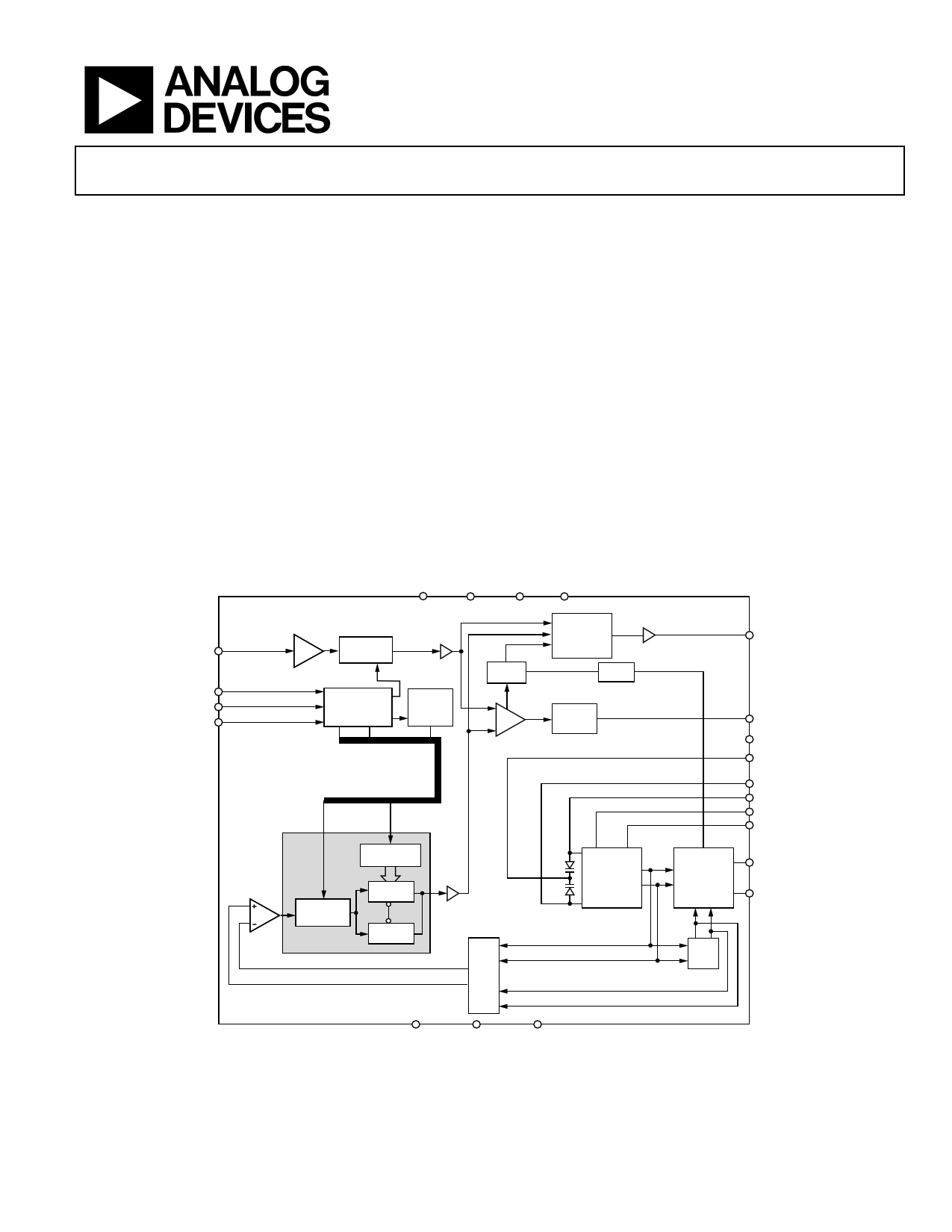
FUNCTIONAL BLOCK DIAGRAM
AVDD
DVDD
RSET
CE
REFIN
CLK
DATA
LE
ADF4360-7
14-BIT R
COUNTER
24-BIT
DATA REGISTER
24-BIT
FUNCTION
LATCH
LOCK
DETECT
MULTIPLEXER
MUTE
CHARGE
PUMP
PHASE
COMPARATOR
INTEGER
REGISTER
PRESCALER
P/P+1
N = (BP + A)
13-BIT B
COUNTER
LOAD
LOAD
5-BIT A
COUNTER
VCO
CORE
DIVSEL = 1
MUXOUT
OUTPUT
STAGE
CP
VVCO
VTUNE
L1
L2
CC
CN
RFOUTA
RFOUTB
÷2
AGND
DIVSEL = 2
DGND
CPGND
Figure 1.
Rev. E
Document Feedback
Information furnished by Analog Devices is believed to be accurate and reliable. However, no re-
sponsibility is assumed by Analog Devices for its use, nor for any infringements of patents or other
rights of third parties that may result from its use. Specifications subject to change without notice. No
license is granted by implication or otherwise under any patent or patent rights of Analog Devices.
Trademarksandregisteredtrademarksarethepropertyoftheirrespectiveowners.
One Technology Way, P.O. Box 9106, Norwood, MA 02062-9106, U.S.A.
Tel: 781.329.4700 ©2004–2016 Analog Devices, Inc. All rights reserved.
Technical Support
www.analog.com
1 page 
ADF4360-7
Data Sheet
Parameter
RF OUTPUT CHARACTERISTICS5
Maximum VCO Output Frequency
Minimum VCO Output Frequency
VCO Output Frequency
VCO Frequency Range
VCO Sensitivity
Lock Time6
Frequency Pushing (Open Loop)
Frequency Pulling (Open Loop)
Harmonic Content (Second)
Harmonic Content (Third)
Output Power5, 7
Output Power Variation
VCO Tuning Range
NOISE CHARACTERISTIC5
VCO Phase-Noise Performance8
Synthesizer Phase-Noise Floor9
In-Band Phase Noise10, 11
RMS Integrated Phase Error12
Spurious Signals due to PFD Fre-
quency11, 13
B Version Unit
1800
350
490/585
1.2
12
400
6
15
−19
−9
−14/−5
±3
1.25/2.5
MHz
MHz
MHz min/max
Ratio
MHz/V typ
µs typ
MHz/V typ
kHz typ
dBc typ
dBc typ
dBm typ
dB typ
V min/max
−116
−138
−144
−148
−172
−163
−147
−92
0.3
−70
dBc/Hz typ
dBc/Hz typ
dBc/Hz typ
dBc/Hz typ
dBc/Hz typ
dBc/Hz typ
dBc/Hz typ
dBc/Hz typ
Degrees typ
dBc typ
Test Conditions/Comments
ICORE = 5 mA. Depending on L. See the Choosing the Correct
Inductance Value section.
L1, L2 = 13 nH. See the Choosing the Correct Inductance Value
section for other frequency values.
FMAX/FMIN
L1, L2 = 13 nH. See the Choosing the Correct Inductance Value
section for other sensitivity values.
To within 10 Hz of final frequency.
Into 2.00 VSWR load.
Programmable in 3 dB steps. See Table 7.
For tuned loads, see Output Matching section.
At 100 kHz offset from carrier.
At 1 MHz offset from carrier.
At 3 MHz offset from carrier.
At 10 MHz offset from carrier.
At 25 kHz PFD frequency.
At 200 kHz PFD frequency.
At 8 MHz PFD frequency.
At 1 kHz offset from carrier.
100 Hz to 100 kHz.
Level of Unlocked Signal with
MTLD Enabled
−44
dBm typ
1 Operating temperature range is –40°C to +85°C.
2 Guaranteed by design. Sample tested to ensure compliance.
3 ICP is internally modified to maintain constant loop gain over the frequency range.
4 TA = 25°C; AVDD = DVDD = VVCO = 3.3 V; P = 32.
5 Unless otherwise stated, these characteristics are guaranteed for VCO core power = 5 mA. L1, L2 = 13 nH, 470 Ω resistors to GND in parallel with L1, L2.
6 Jumping from 490 MHz to 585 MHz. PFD frequency = 200 kHz; loop bandwidth = 10 kHz.
7 Using 50 Ω resistors to VVCO, into a 50 Ω load. For tuned loads, see the Output Matching section.
8 The noise of the VCO is measured in open-loop conditions.
9 The synthesizer phase-noise floor is estimated by measuring the in-band phase noise at the output of the VCO and subtracting 20 log N (where N is the N divider value).
10 The phase noise is measured with the EV-ADF4360-7EB1Z Evaluation Board and the HP 8562E Spectrum Analyzer. The Spectrum Analyzer provides the REFIN for the
synthesizer; offset frequency = 1 kHz.
11 fREFIN = 10 MHz; fPFD = 200 kHz; N = 2500; loop B/W = 10 kHz.
12 fREFIN = 10 MHz; fPFD = 1 MHz; N = 500; loop B/W = 25 kHz.
13 The spurious signals are measured with the EV-ADF4360-7EB1Z Evaluation Board and the HP 8562E Spectrum Analyzer. The Spectrum Analyzer provides the REFIN for
the synthesizer; fREFOUT = 10 MHz at 0 dBm.
Rev. E | Page 4 of 28
5 Page 
ADF4360-7
Data Sheet
CIRCUIT DESCRIPTION
REFERENCE INPUT SECTION
The reference input stage is shown in Figure 16. SW1 and SW2
are normally closed switches. SW3 is normally open. When
power-down is initiated, SW3 is closed, and SW1 and SW2 are
opened. This ensures that there is no loading of the REFIN pin
on power-down.
POWER-DOWN
CONTROL
NC 100k
REFIN NC
SW2
SW1
SW3
NO
TO R COUNTER
BUFFER
Figure 16. Reference Input Stage
PRESCALER (P/P + 1)
The dual-modulus prescaler (P/P + 1), along with the A and B
counters, enables the large division ratio, N, to be realized
(N = BP + A). The dual-modulus prescaler, operating at CML
levels, takes the clock from the VCO and divides it down to a
manageable frequency for the CMOS A and B counters. The
prescaler is programmable. It can be set in software to 8/9,
16/17, or 32/33 and is based on a synchronous 4/5 core. There is
a minimum divide ratio possible for fully contiguous output
frequencies; this minimum is determined by P, the prescaler
value, and is given by (P2 − P).
A AND B COUNTERS
The A and B CMOS counters combine with the dual-modulus
prescaler to allow a wide range division ratio in the PLL feed-
back counter. The counters are specified to work when the
prescaler output is 300 MHz or less. Thus, with a VCO
frequency of 2.5 GHz, a prescaler value of 16/17 is valid, but a
value of 8/9 is not valid. At fundamental VCO frequencies less
than 700 MHz, a value of 8/9 is best.
Pulse Swallow Function
The A and B counters, in conjunction with the dual-modulus
prescaler, make it possible to generate output frequencies that
are spaced only by the reference frequency divided by R. The
VCO frequency equation is
fVCO P B A f REFIN /R
where:
fVCO is the output frequency of the VCO.
P is the preset modulus of the dual-modulus prescaler
(8/9 or 16/17).
B is the preset divide ratio of the binary 13-bit counter (3 to 8191).
A is the preset divide ratio of the binary 5-bit swallow counter
(0 to 31).
fREFIN is the external reference frequency oscillator.
FROM VCO
N = BP + A
PRESCALER
P/P+1
MODULUS
CONTROL
13-BIT B
COUNTER
LOAD
LOAD
5-BIT A
COUNTER
TO PFD
N DIVIDER
Figure 17. A and B Counters
R COUNTER
The 14-bit R counter allows the input reference frequency to
be divided down to produce the reference clock to the phase
frequency detector (PFD). Division ratios from 1 to 16,383 are
allowed.
PFD AND CHARGE PUMP
The PFD takes inputs from the R counter and N counter
(N = BP + A) and produces an output proportional to the phase
and frequency difference between them. Figure 18 is a simpli-
fied schematic. The PFD includes a programmable delay ele-
ment that controls the width of the antibacklash pulse. This
pulse ensures that there is no dead zone in the PFD transfer
function and minimizes phase noise and reference spurs. Two
bits in the R counter latch, ABP2 and ABP1, control the width
of the pulse (see Table 9).
HI
R DIVIDER
UP
D1 Q1
U1
CLR1
VP CHARGE
PUMP
PROGRAMMABLE
DELAY
U3
ABP1
ABP2
HI
N DIVIDER
CLR2
DOWN
D2 Q2
U2
CP
CPGND
R DIVIDER
N DIVIDER
CP OUTPUT
Figure 18. PFD Simplified Schematic and Timing (In Lock)
Rev. E | Page 10 of 28
11 Page | ||
| Páginas | Total 29 Páginas | |
| PDF Descargar | [ Datasheet ADF4360-7.PDF ] | |
Hoja de datos destacado
| Número de pieza | Descripción | Fabricantes |
| ADF4360-0 | Integrated Synthesizer and VCO | Analog Devices |
| ADF4360-1 | Integrated Synthesizer and VCO | Analog Devices |
| ADF4360-2 | Integrated Synthesizer and VCO | Analog Devices |
| ADF4360-3 | Integrated Synthesizer and VCO | Analog Devices |
| Número de pieza | Descripción | Fabricantes |
| SLA6805M | High Voltage 3 phase Motor Driver IC. |
Sanken |
| SDC1742 | 12- and 14-Bit Hybrid Synchro / Resolver-to-Digital Converters. |
Analog Devices |
|
DataSheet.es es una pagina web que funciona como un repositorio de manuales o hoja de datos de muchos de los productos más populares, |
| DataSheet.es | 2020 | Privacy Policy | Contacto | Buscar |