|
|
PDF EM5303 Data sheet ( Hoja de datos )
| Número de pieza | EM5303 | |
| Descripción | 5V 12V Synchronous Buck PWM Controller | |
| Fabricantes | CYStech Electronics | |
| Logotipo |  |
|
Hay una vista previa y un enlace de descarga de EM5303 (archivo pdf) en la parte inferior de esta página. Total 12 Páginas | ||
|
No Preview Available !
CYStech Electronics Corp.
5V/12V Synchronous Buck PWM Controller
EM5303/A
Spec. No. : C551QP
Issued Date : 2010.10.25
Revised Date :
Page No. : 1/12
General Description
EM5303/A is a synchronous rectified PWM controller operating with 5V or 12V supply voltage. This
device operates at 200/300 kHz and provides an optimal level of integration to reduce size and cost of the
power supply.
This part includes internal soft start, internal compensation networks, over current protection, under
voltage protection, and shutdown function. This part is available in PSOP-8 package.
Features
z Operate from 5V to 12V Voltage Supply
z 0.6V VREF with 1.5% Accuracy
z Voltage Mode PWM Control
z 200kHz or 300kHz Fixed Frequency Oscillator
z 0% to 80% Duty Cycle
z Internal Soft Start
z Over Current Protection
z Integrated Bootstrap Diode
z Adaptive Non-Overlapping Gate Driver
z Under Voltage Protection
z Over Voltage Protection
Applications
z Notebook & Netbook
z Graphic Cards & MB
z Low Voltage Logic Supplies
Ordering Information
Part Number
EM5303QP
EM5303AQP
Package
PSOP-8
PSOP-8
Frequency
200kHz
300kHz
EM5303QP
CYStek Product Specification
http://www.Datasheet4U.com
1 page 
CYStech Electronics Corp.
Spec. No. : C551QP
Issued Date : 2010.10.25
Revised Date :
Page No. : 5/12
PWM Controller Gate Drivers
Upper Gate Sourcing Current IUG_SRC
VBOOT - VPHASE = 12V,
VBOOT - VUGATE = 6V
Upper Gate Sinking Current
IUG_SNK
VBOOT - VPHASE = 12V,
VUGATE – VPHASE = 6V
Upper Gate RDS(ON) Sinking
RUG_SNK
VBOOT - VPHASE = 12V,
VUGATE – VPHASE = 0.1V
Lower Gate Sourcing Current ILG_SRC VCC – VLGATE = 6V
Lower Gate Sinking Current ILG_SNK VLGATE = 6V
Lower Gate RDS(ON) Sinking
PHASE Falling to LGATE Rising
Delay
LGATE Falling to UGATE Rising
Delay
RLG_SNK
VLGATE = 0.1V
VCC = 12V; VPHASE < 1.2V to
VLGATE > 1.2V
VCC = 12V; VLGATE < 1.2V to
(VUGATE - VPHASE) > 1.2V
Reference Voltage
Nominal Feedback Voltage VFB
Enable Voltage
EN Enable Threshold
VEN
Protection section
FB Under Voltage Protection VFB_UVP FB falling
FB Over Voltage Protection VFB_OVP FB rising
VCC Over Voltage Protection VCC_OVP
Over Current Threshold
VOCP
Soft-Start Interval
TSS
Temperature Shutdown
TSD Guaranteed by Design
2 -1
A
2 1.5
A
2 24Ω
4 -1
A
4 1.5
A
4 24Ω
30 90 nS
30 90 ns
6 0.591 0.6 0.609 V
7 0.3 0.35 V
6 55 65 75 %
6 115 130 145 %
5 16 17 18 V
-425 -375 -325 mV
2.4 3.6 5.4 mS
150 165
℃
Note 1.
Note 2.
Note 3.
Note 4.
Note 5.
Stresses listed as the above “Absolute Maximum Ratings” may cause permanent damage to the device. These are for
stress ratings. Functional operation of the device at these or any other conditions beyond those indicated in the
operational sections of the specifications is not implied. Exposure to absolute maximum rating conditions for extended
periods may remain possibility to affect device reliability.
θJA is measured in the natural convection at TA=25oC on a 4-layers high effective thermal conductivity test board with
minimum copper area of JEDEC 51-7 thermal measurement standard. The case point of θJC is on the expose pad for
PSOP-8 package.
θJA PSOP-8 packages is 52°C /W on JEDEC 51-7 (4 layers,2S2P) thermal test board with 50mm2 copper area.
Devices are ESD sensitive. Handling precaution is recommended.
The device is not guaranteed to function outside its operating conditions.
EM5303QP
CYStek Product Specification
5 Page 
CYStech Electronics Corp.
Spec. No. : C551QP
Issued Date : 2010.10.25
Revised Date :
Page No. : 11/12
Recommended wave soldering condition
Product
Peak Temperature
Pb-free devices
260 +0/-5 °C
Soldering Time
5 +1/-1 seconds
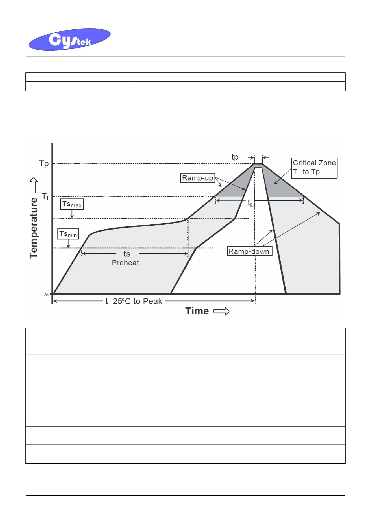
Recommended temperature profile for IR reflow
Profile feature
Sn-Pb eutectic Assembly
Pb-free Assembly
Average ramp-up rate
(Tsmax to Tp)
3°C/second max.
3°C/second max.
Preheat
−Temperature Min(TS min)
−Temperature Max(TS max)
−Time(ts min to ts max)
100°C
150°C
60-120 seconds
150°C
200°C
60-180 seconds
Time maintained above:
−Temperature (TL)
− Time (tL)
183°C
60-150 seconds
217°C
60-150 seconds
Peak Temperature(TP)
240 +0/-5 °C
260 +0/-5 °C
Time within 5°C of actual peak
temperature(tp)
10-30 seconds
20-40 seconds
Ramp down rate
6°C/second max.
6°C/second max.
Time 25 °C to peak temperature
6 minutes max.
8 minutes max.
Note : All temperatures refer to topside of the package, measured on the package body surface.
EM5303QP
CYStek Product Specification
11 Page | ||
| Páginas | Total 12 Páginas | |
| PDF Descargar | [ Datasheet EM5303.PDF ] | |
Hoja de datos destacado
| Número de pieza | Descripción | Fabricantes |
| EM5301 | PWM Controller | Excelliance MOS |
| EM5301F | PWM Controller | Excelliance MOS |
| EM5301G | PWM Controller | Excelliance MOS |
| EM5302 | PWM Controller | Excelliance MOS |
| Número de pieza | Descripción | Fabricantes |
| SLA6805M | High Voltage 3 phase Motor Driver IC. |
Sanken |
| SDC1742 | 12- and 14-Bit Hybrid Synchro / Resolver-to-Digital Converters. |
Analog Devices |
|
DataSheet.es es una pagina web que funciona como un repositorio de manuales o hoja de datos de muchos de los productos más populares, |
| DataSheet.es | 2020 | Privacy Policy | Contacto | Buscar |
