|
|
PDF TA65N14A10 Data sheet ( Hoja de datos )
| Número de pieza | TA65N14A10 | |
| Descripción | Advanced Pulse Power Device | |
| Fabricantes | Solidtron | |
| Logotipo |  |
|
Hay una vista previa y un enlace de descarga de TA65N14A10 (archivo pdf) en la parte inferior de esta página. Total 5 Páginas | ||
|
No Preview Available !
SMCT TA65N14A10
Advanced Pulse Power Device
N-MOS VCS, ThinPakTM
Description
This voltage controlled Solidtron (VCS) discharge switch utilizes
an n-type MOS-Controlled Thyristor mounted on a ThinPakTM,
ceramic "chip-scale" hybrid.
The VCS features the high peak current capability and low On-
state voltage drop common to SCR thyristors combined with
extremely high dI/dt capability. This semiconductor is intended
for the control of high power circuits with the use of very small
amounts of input energy and is ideally suited for capacitor
discharge applications.
The ThinPakTM Package is a perforated, metalized ceramic
substrate attached to the silicon using 302oC solder. An epoxy
underfill is applied to protect the high voltage termination from
debris. All exterior metal surfaces are tinned with 63pb/37sn
solder providing the user with a circuit ready part. It's small size
and low profile make it extremely attractive to high dI/dt
applications where stray series inductance must be kept to a
minimum.
Features
l 1400V Peak Off-State Voltage
l 65A Continuous Rating
l 6kA Surge Current Capability
l >100kA/uSec dI/dt Capability
l <150nSec Turn-On Delay
l Low On-State Voltage
l MOS Gated Control
l Low Inductance Package
Package
Gate Bond Area
Anode
Bond Area
Schematic Symbol
Gate (G)
Gate Return (GR)
Gate Return
Bond Area
Cathode Bond Area
ThinPakTM
Anode (A)
Cathode (K)
Absolute Maximum Ratings
Peak Off-State Voltage
Peak Reverse Voltage
Off-State Rate of Change of Voltage Immunity
Continuous Anode Current at 110oC
Repetitive Peak Anode Current (Pulse Width=1uSec)
Rate of Change of Current
Continuous Gate-Cathode Voltage
Peak Gate-Cathode Voltage
Minimum Negative Gate-Cathode Voltage Required for Garanteed Off-State
Maximum Junction Temperature
Maximum Soldering Temperature (Installation)
SYMBOL
VDRM
VRRM
dv/dt
IA110
IASM
dI/dt
VGKS
VGKM
VGK(OFF-MIN)
TJM
VALUE
1400
-5
5000
65
6000
125
+/-20
+/-25
-5
150
260
UNITS
V
V
V/uSec
A
A
kA/uSec
V
V
V
oC
oC
This SILICON POWER product is protected by one or more of the following U.S. Patents:
5,521,436
5,585,310
5,248,901
5,366,932
5,497,013
5,532,635
5,446,316
5,557,656
5,564,226
5,517,058
4,814,283
5,135,890
5,105,536
5,777,346
5,446,316
5,577,656
5,473,193
5,166,773
5,209,390
5,139,972
5,103,290
5,028,987
5,304,847
5,569,957
4,958,211
5,111,268
5,260,590
5,350,935
5,640,300
5,184,206
5,206,186
5,757,036
5,777,346
5,995,349
4,801,985
4,476,671
4,857,983
4,888,627
4,912,541
5,424,563
5,399,892
5,468,668
5,082,795
4,980,741
4,941,026
4,927,772
4,739,387
4,648,174
4,644,637
4,374,389
4,750,666
4,429,011
5,293,070
http://www.Datasheet4U.com
1 page 
SMCT TA65N14A10
Advanced Pulse Power Device
N-MOS VCS, ThinPakTM
Application Notes
A1. Junction Temperature Calculation
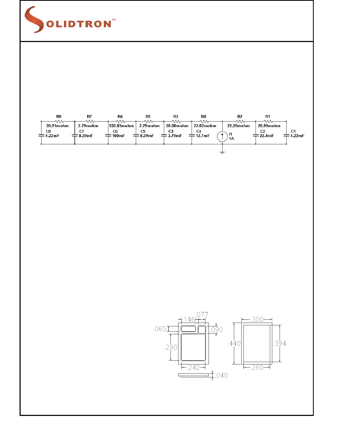
The figure below shows a lump model of the thermal properties of the size 6 thinPak packaged VCS, from the 2-mil solder on
the top of the lid on the left to the 2-mil solder on the bottom of the device on the right. By adding the user's lump model of the
rest of the thermal system the user can calculate the junction and case temperature rise under any operating condition.
Cathode-Gate
(Top) Side
Interface
Device
Junction
Anode
(Bottom) Side
Interface
A2. Calculation of Pulses to Failure for Intermediate/Long Pulse Widths
The user may calculate the Number of Pulses to failure (NF) for long to intermedeiate pulse widths (not covered in the typical
performance curve section) by applying the junction temperature rise (dT), calculated as described in A1, to the formula
NF=(300/dT)9 .
A3. Use of Gate Return Bond Area.
The MCT was designed for high di/dt applications. An independent cathode connection or "Gate Return Bond Area" was
provided to minimize the effects of rapidly changing Anode-Cathode current on the Gate control voltage, (V=L*di/dt). It is
therefore, critcal that the user utilize the Gate Return Bond Area as the point at which the gate driver reference (return) is
attached to the VCS device.
Packaging and Handling
1. All metal surfaces are tinned using 63pb/37sn
solder.
2. Installation reflow temperature should not exceed
260oC or internal package degradation may result.
3. Package may be cooled from either top or bottom
(See Figures 7 & A1 Application Notes.)
4. As with all MOS gated devices, proper handling
procedures must be observed to prevent electrostatic
discharge which may result in permanant damage to
the gate of the device
Package Dimensions
Top
Cathode-Gate
Bottom
Anode
Side
5 Page | ||
| Páginas | Total 5 Páginas | |
| PDF Descargar | [ Datasheet TA65N14A10.PDF ] | |
Hoja de datos destacado
| Número de pieza | Descripción | Fabricantes |
| TA65N14A10 | Advanced Pulse Power Device | Solidtron |
| Número de pieza | Descripción | Fabricantes |
| SLA6805M | High Voltage 3 phase Motor Driver IC. |
Sanken |
| SDC1742 | 12- and 14-Bit Hybrid Synchro / Resolver-to-Digital Converters. |
Analog Devices |
|
DataSheet.es es una pagina web que funciona como un repositorio de manuales o hoja de datos de muchos de los productos más populares, |
| DataSheet.es | 2020 | Privacy Policy | Contacto | Buscar |
