|
|
|
PDF NCV7342 Data sheet ( Hoja de datos )
| Número de pieza | NCV7342 | |
| Descripción | High Speed Low Power CAN Transceiver | |
| Fabricantes | ON Semiconductor | |
| Logotipo | ||
Hay una vista previa y un enlace de descarga de NCV7342 (archivo pdf) en la parte inferior de esta página. Total 15 Páginas | ||
|
No Preview Available !
NCV7342
High Speed Low Power CAN
Transceiver
Description
The NCV7342 CAN transceiver is the interface between a
controller area network (CAN) protocol controller and the physical
bus and may be used in both 12 V and 24 V systems. The transceiver
provides differential transmit capability to the bus and differential
receive capability to the CAN controller.
The NCV7342 is an addition to the CAN high−speed transceiver
family complementing NCV734x CAN stand−alone transceivers and
previous generations such as AMIS42665, AMIS3066x, etc.
Due to the wide common−mode voltage range of the receiver inputs
and other design features, the NCV7342 is able to reach outstanding
levels of electromagnetic susceptibility (EMS). Similarly, extremely
low electromagnetic emission (EME) is achieved by the excellent
matching of the output signals.
Features
• Compatible with the ISO 11898−2, ISO 11898−5 Standards
• High Speed (up to 1 Mbps)
• VIO Pin on NCV7342−3 Version Allowing Direct Interfacing with
3 V to 5 V Microcontrollers
• VSPLIT Pin on NCV7342−0 Version for Bus Common Mode
Stabilization
• Very Low Current Consumption in Standby Mode with Wake−up via
the Bus
• Excellent Electromagnetic Susceptibility (EMS) Level Over Full
Frequency Range. Very Low Electromagnetic Emissions (EME) Low
EME Also Without Common Mode (CM) Choke
• Bus Pins Protected Against >15 kV System ESD Pulses
• Transmit Data (TxD) Dominant Time−out Function
• Bus Dominant Time−out function in Standby Mode
• Under All Supply Condition the Chip Behaves Predictably
• No Disturbance of the Bus Lines with an Unpowered Node
• Thermal Protection
• Bus Pins Protected Against Transients in an Automotive
Environment
• Bus Pins Short Circuit Proof to Supply Voltage and Ground
• These are Pb−Free Devices
Quality
• Wettable Flank Package for Enhanced Optical Inspection
• NCV Prefix for Automotive and Other Applications Requiring
Unique Site and Control Change Requirements; AEC−Q100
Qualified and PPAP Capable
Typical Applications
• Automotive
• Industrial Networks
www.onsemi.com
8
1
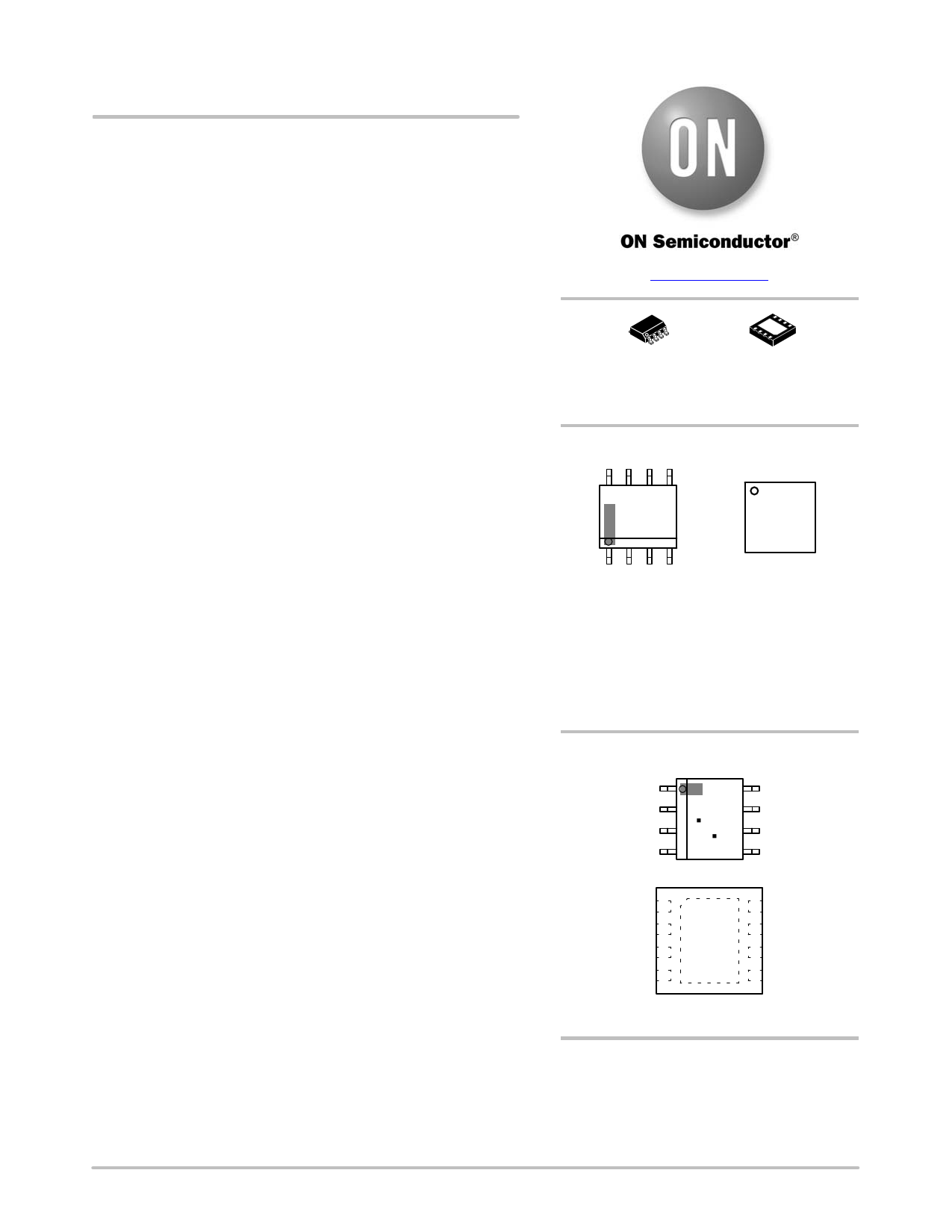
SOIC−8
D SUFFIX
CASE 751AZ
1
DFN8
MW SUFFIX
CASE 506CS
MARKING DIAGRAMS
8
NV7342−x
ALYW G
G
1
1
NV7342−x
ALYWG
G
NV7342−x= Specific Device Code
x = 0 or 3
A = Assembly Location
L = Wafer Lot
Y = Year
W = Work Week
G = Pb−Free Package
(Note: Microdot may be in either location)
PIN ASSIGNMENTS
1
TxD
2
GND
3
VCC 4
RxD
8
STB
7
CANH
6
CANL
5
VSPLIT (−0)
VIO (−3)
TxD 1
GND 2
VCC 3
RxD 4
EP Flag
8 STB
7 CANH
6 CANL
5 VIO
(Top Views)
ORDERING INFORMATION
See detailed ordering and shipping information in the package
dimensions section on page 13 of this data sheet.
© Semiconductor Components Industries, LLC, 2016
February, 2016 − Rev. 3
1
Publication Order Number:
NCV7342/D
1 page 
NCV7342
TYPICAL APPLICATION
VBAT
5V−reg
3V−reg
VIO
Micro
Controller
GND
VIO
5
STB
8
VCC
3
7
CANH
RxD NCV7342−3
4
RLT = 60 W
CLT = 4.7 nF CAN
BUS
TxD
1
6 CANL
2 RLT = 60 W
GND
RB20120816
Figure 3. Application Diagram NCV7342−3
VBAT
IN OUT
5V−reg
RB20120816
VCC
Micro
Controller
GND
STB
8
RxD
4
TxD
1
VCC
3
RLT = 60 W
7
CANH
VSPLIT
5
CLT = 4.7 nF
CAN
BUS
6
2
GND
CANL
RLT = 60 W
Figure 4. Application Diagram NCV7342−0
Table 2. PIN FUNCTION DESCRIPTION
Pin Name
Description
1 TxD Transmit data input; Low input Ù dominant driver; internal pull−up current
2
GND
Ground
3 VCC Supply voltage
4 RxD Receive data output; dominant transmitter Ù Low output
5 VIO Input/Output pins supply voltage. On NCV7342−3 only
5
VSPLIT
Common−mode stabilization output. On NCV7342−0 only
6
CANL
Low−level CAN bus line (Low in dominant mode)
7
CANH
High−level CAN bus line (High in dominant mode)
8 STB Standby mode control input
EP Exposed Pad Connect to GND or left floating
www.onsemi.com
5
5 Page 
NCV7342
Table 6. CHARACTERISTICS
VCC = 4.5 V to 5.5 V; VIO = 2.8V to 5.5 V (Note 10); TJ = −40 to +150°C; RLT = 60 W unless specified otherwise. On chip versions
without VIO pin reference voltage for all digital inputs and outputs is VCC instead of VIO.
Symbol
Parameter
Conditions
Min Typ
Max Unit
VIO SUPPLY VOLTAGE (Pin VIO) Only for NCV7342−3 version
IIONM
Supply current on pin VIO
Normal mode
Dominant; VTxD = 0 V
Recessive; VTxD = VIO
VUVDVIO
Undervoltage detection voltage on
VIO pin
THERMAL SHUTDOWN
mA
0.30 0.70
1.10
0.29 0.44
0.68
1.3 2.7 V
TJ(SD)
Shutdown junction temperature
TIMING CHARACTERISTICS (See Figure 7 and 8)
junction temperature rising
160 180 200 °C
td(TxD−BUSon)
Delay TxD to bus active
Ci = 100 pF between CANH to
CANL
60
ns
td(TxD−BUSoff)
Delay TxD to bus inactive
Ci = 100 pF between CANH to
CANL
30
ns
td(BUSon−RxD)
Delay bus active to RxD
CRxD = 15 pF
60 ns
td(BUSoff−RxD)
Delay bus inactive to RxD
CRxD = 15 pF
70 ns
tpd_dr
Propagation delay TxD to RxD Ci = 100 pF between CANH to 50 100 230 ns
dominant to recessive transition
CANL, CRxD = 15 pF
See Figure 8
tpd_rd
Propagation delay TxD to RxD Ci = 100 pF between CANH to 50 120 230 ns
recessive to dominant transition
CANL, CRxD = 15 pF
See Figure 8
td(stb−nm)
Delay standby mode to normal
mode
47 ms
tWake
tdwakerd
Dominant time for wake−up via bus
Delay to flag wake event
(recessive to dominant transitions)
See Figure 5
Valid bus wake−up event,
CRxD = 15 pF
0.5 2.1 5 ms
1 3.5 10 ms
tdwakedr
Delay to flag end of wake event
(dominant to recessive transition)
See Figure 5
Valid bus wake−up event,
CRxD = 15 pF
0.5 2.6 6 ms
tWake(RxD)
Minimum pulse width on RxD
See Figure 5
5 ms tWake
CRxD = 15 pF
0.5
ms
tdom(TxD)
TxD dominant time for time out
VTxD = 0 V
1.3 5 ms
tdom(bus)
Bus dominant time out
Standby mode
1.3 5 ms
10. Only version NCV7342−3 has VIO supply pin. In NCV7342−0 this supply is provided from VCC pin.
11. Not tested in production. Guaranteed by design and prototype evaluation.
12. In case VIO > VCC, the limit is VIO + 0.3 V
Product parametric performance is indicated in the Electrical Characteristics for the listed test conditions, unless otherwise noted. Product
performance may not be indicated by the Electrical Characteristics if operated under different conditions.
www.onsemi.com
11
11 Page | ||
| Páginas | Total 15 Páginas | |
| PDF Descargar | [ Datasheet NCV7342.PDF ] | |
Hoja de datos destacado
| Número de pieza | Descripción | Fabricantes |
| NCV7340 | High Speed Low Power CAN Transceiver | ON Semiconductor |
| NCV7341 | High Speed Low Power CAN Transceiver | ON Semiconductor |
| NCV7342 | High Speed Low Power CAN Transceiver | ON Semiconductor |
| NCV7349 | High Speed Low Power CAN Transceiver | ON Semiconductor |
| Número de pieza | Descripción | Fabricantes |
| SLA6805M | High Voltage 3 phase Motor Driver IC. |
Sanken |
| SDC1742 | 12- and 14-Bit Hybrid Synchro / Resolver-to-Digital Converters. |
Analog Devices |
|
DataSheet.es es una pagina web que funciona como un repositorio de manuales o hoja de datos de muchos de los productos más populares, |
| DataSheet.es | 2020 | Privacy Policy | Contacto | Buscar |