|
|
|
PDF NX2415 Data sheet ( Hoja de datos )
| Número de pieza | NX2415 | |
| Descripción | TWO PHASE SYNCHRONOUS PWM CONTROLLER | |
| Fabricantes | NEXSEM | |
| Logotipo | ||
Hay una vista previa y un enlace de descarga de NX2415 (archivo pdf) en la parte inferior de esta página. Total 22 Páginas | ||
|
No Preview Available !
NEXSEM
Evaluation board available.
NX2415
TWO PHASE SYNCHRONOUS PWM CONTROLLER WITH
INTEGRATED FET DRIVER AND DIFFERENTIAL CURRENT SENSE
PRELIMINARY DATA SHEET
Pb Free Product
DESCRIPTION
FEATURES
The NX2415 is a two-phase PWM controller with inte- n Differential inductor DCR sensing eliminates the
grated FET driver designed for low voltage high current
application. The two phase synchronous buck converter
offers ripple cancelation for both input and output. The
NX2415 uses differential remote sensing using either
current sense resistor or inductor DCR sensing to achieve
accurate current matching between the two channels.
n
n
n
n
n
problem with layout parasitic
External programmable voltage droop
Low Impedance On-board Drivers
Hiccup current limit
Power Good for power sequencing
Enable Signal allows external shutdown as well as
Differential sensing eliminates the error caused by PCB
board trace resistance that is otherwise is present when
using a single ended voltage sensing. In addition the
NX2415 offers high drive current capability especially for
n
n
n
programming the BUS voltage start up threshold
Programmable frequency
Prebias start up
Over voltage protection without negative spike at
keeping the synchronous MOSFET off during SW node output
transition, accurate programmable droop allowing to re- n Pb-free and RoHS compliant
duce number of output capacitors, accurate enable cir-
APPLICATIONS
cuit provides programmable start up point for Bus volt- n Graphic card High Current Vcore Supply
age, PGOOD output, programmable switching frequencyn High Current +40A on board DC to DC converter
and hiccup current limiting circuitry.
applications
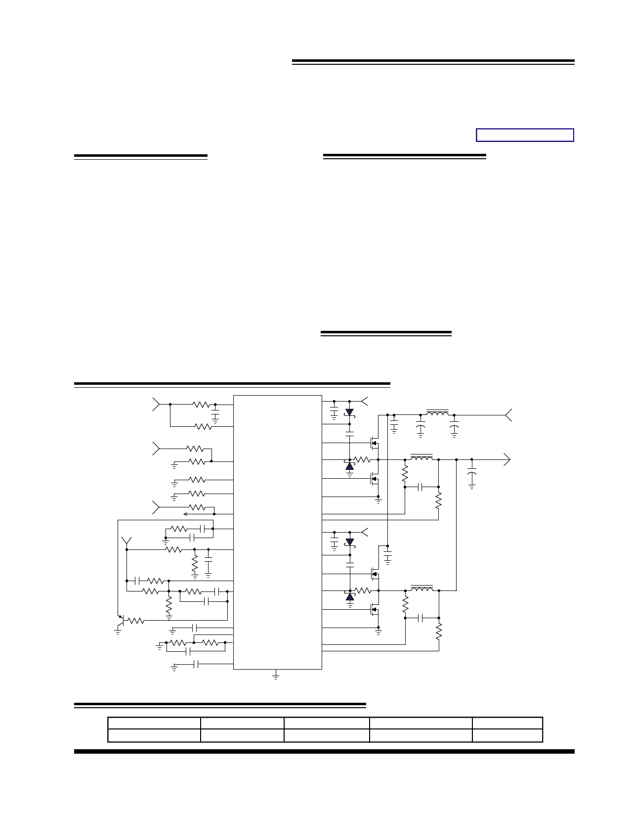
TYPICAL APPLICATION
+5V
10 31
VCC
1uF
10k 30
EN
+12V
6.49k
1.65k
29 ENBUS
+5V
op
45.3k
10k
7 DROOP
2 RT
28 PGOOD
VOUT
11 CSCOMP
430 220nF
1.8nF 3.92k
10k
2N3906
20k
2.2nF
10k
20k
5.62k
3 PGSEN
1nF
5 FB
6.8nF
6 VCOMP
150pF
PVCC1 23 1uF
+5V
1uH
BST1 24
HDRV1 25
SW1 26
2 x 10uF
180uF
0.22uF M1
2.15 0.68uH
LDRV1 22
M2 620
1uF
100uF
VIN1
+12V
VOUT
+1.2V/50A
2 x (1000uF,7mohm ESR)
PGND1 21
CS+1 9
CS-1 10
PVCC2 18
1uF
+5V
620
17
BST2
16
HDRV2
15
SW2
19
LDRV2
0.22uF
2.15
10uF
M3
0.68uH
M4 620
1uF
1k
180k
10nF
100k
4
8
VP
OCP
1 VREF
10nF
20
PGND2
CS+2 12
CS-2 13
1nF 14 IOUT AGND
32
620
Figure1 - Typical application of NX2415
ORDERING INFORMATION
Device
NX2415CMTR
Temperature
0 to 70oC
Package
MLPQ-32L
Frequency
200kHz to 1MHz
Pb-Free
Yes
Rev.4.8
05/06/08
www.nexsem.com
1
Free Datasheet http://www.Datasheet4U.com
1 page 
NEXSEM
NX2415
PIN DESCRIPTIONS
PIN #
SYMBOL
PIN DESCRIPTION
31 VCC IC’s supply voltage. This pin biases the internal logic circuits. A minimum 1uF
ceramic capacitor is recommended to connect from this pin to ground plane.
25, HDRV1, High side gate driver outputs.
16 HDRV2
22, LDRV1, Low side gate driver outputs.
19 LDRV2
30 EN This pin is used to remotely turn off the controller. The pin has a threshold
voltage of 0.6 volts.
24, 17
BST1,BST2 These pins supplies voltage to high side FET drivers.
26,15
SW1,SW2 These pins are connected to the source pins of the upper fets.
23, PVCC1, These pins provide the supply voltage for the lower MOSFET drivers.
18 PVCC2
28 PGOOD This pin is an open collector output. If used, it should be pulled to 5V with a
resistor greater than or equal to 10k, otherwise it my be left open. Any fault or
under voltage on the enable pins will cause the signal to be pulled low.
4 VP Input to the positive pin of the error amplifier. A resistor is connected from the
output of the DAC to this pin. Place a small capacitor from this pin to GND to
filter any noise.
5 FB This pin is the error amplifier inverting input. It is connected to the output voltage
via a voltage divider.
2 RT This pin programs the internal oscillator frequency using a resistor from this pin to
ground. The frequency of each phase is 1/2 of this frequency.
9,12 CS+1,CS+2 Positive input of the differential current sense amplifiers. It is connected directly
to the RC junction of the respective phase’s output inductor.
10,13
CS-1,CS-2 Negative input of the differential current sense amplifiers. It is connected directly
to the negative side of the respective phase’s output inductor.
11 CSCOMP The output of the transconductance op amp for current balance circuit. An
external RC is connected from this pin to GND to stabilize the current loop.
6 VCOMP This is the output pin of the error amplifier. The compensation network connec-
tion.
7
Rev.4.8
05/06/08
DROOP
A resistor from this pin to ground programs an internal current source that is fed
into the FB pin. This current source is proportional to the output current of the
regulator. The product of this current times the external resistor RFB provides a
droop voltage.
www.nexsem.com
5
FreeDatasheethttp://www.Datasheet4U.com
5 Page 
NEXSEM
NX2415
The transfer function of type III compensator
is given by:
[ ]Ve
VOUT
=
sR2
1
×(C2
+
C1)
×
(1+ sR4 ×C2)× 1+ s(R2 + R3)×C3
(1+
sR4
×
C2
C2
×
+
C1
C1
)
×
(1+
sR3
×
C3
)
6. Calculate R4 by choosing FO=40kHz.
R4 =
VOSC
Vin
×
2 × π × FO × LEFF
ESR
×
R2
R2
× R3
+ R3
= 1V × 2 × π × 40kHz × 0.34uH × 10kΩ × 3.92kΩ
12V 3.5mΩ 10kΩ + 3.92kΩ
=5.73kΩ
Use the same power stage requirement as demo
board. The crossover frequency has to be selected as
F <F <F , and usually F <=1/10~1/5F .
LC ESR O
OS
1.Calculate the location of LC double pole F
LC
and ESR zero F .
ESR
FLC = 2× π ×
1
LEFF × COUT
=1
2× π × 0.34uH× 2000uF
= 6.1kHz
FESR
=
1
2 × π × ESR × COUT
=1
2 × π × 3.5mΩ × 2000uF
= 22.7kHz
2.Set R2 equal to10kΩ.
R1=
R2 ×
VOUT
VREF
-VREF
= 10kΩ × 0.8V
1.2V-0.8V
= 20kΩ
Choose R1= 20kΩ.
3. Calculate C3 by setting FZ2 = FLC and Fp1 =FESR.
C3
=
2
×
1
π×
R
2
×( 1
Fz2
-
1
Fp1
)
= 1 ×( 1 - 1 )
2 × π ×10kΩ 6.1kHz 22.7kHz
=1.9nF
Choose C3=1.8nF.
5. Calculate R by equation (13).
3
Choose R4=5.62kΩ.
7. Calculate C2 with zero Fz1 at 75% of the LC
double pole by equation (11).
C2
=
1
2 × π × FZ1 × R4
=1
2 × π × 0.75 × 6.1kHz × 5.62kΩ
= 6.2nF
Choose C =6.8nF.
2
8. Calculate C by equation (14) with pole F at
1 p2
half the switching frequency.
C1
=
2×π
1
× R4
× FP2
=1
2 × π × 5.62kΩ × 200kHz
= 141pF
Choose C1=150pF.
B. Type II compensator design
If the electrolytic capacitors are chosen as power
stage output capacitors, usually the Type II compensa-
tor can be used to compensate the system.
Type II compensator can be realized by simple RC
circuit without feedback as shown in figure 4. R3 and C1
introduce a zero to cancel the double pole effect. C2
introduces a pole to suppress the switching noise. The
following equations show the compensator pole zero lo-
cation and constant gain.
R3
=
1
2 × π × FP1 × C3
=1
2 × π × 22.7kHz ×1.8nF
= 3.89kΩ
Choose R3=3.92kΩ.
Gain= R3
R2
1
Fz = 2 × π × R3 × C1
Fp
≈
1
2 × π × R3
× C2
... (15)
... (16)
... (17)
Rev.4.8
05/06/08
www.nexsem.com
11
Free Datasheet http://www.Datasheet4U.com
11 Page | ||
| Páginas | Total 22 Páginas | |
| PDF Descargar | [ Datasheet NX2415.PDF ] | |
Hoja de datos destacado
| Número de pieza | Descripción | Fabricantes |
| NX2415 | DOT MATRIX PRINTER MANUAL | star |
| NX2415 | TWO PHASE SYNCHRONOUS PWM CONTROLLER | NEXSEM |
| NX2415II | DOT MATRIX PRINTER MANUAL | star |
| Número de pieza | Descripción | Fabricantes |
| SLA6805M | High Voltage 3 phase Motor Driver IC. |
Sanken |
| SDC1742 | 12- and 14-Bit Hybrid Synchro / Resolver-to-Digital Converters. |
Analog Devices |
|
DataSheet.es es una pagina web que funciona como un repositorio de manuales o hoja de datos de muchos de los productos más populares, |
| DataSheet.es | 2020 | Privacy Policy | Contacto | Buscar |