|
|
|
PDF HFBR-2115T Data sheet ( Hoja de datos )
| Número de pieza | HFBR-2115T | |
| Descripción | Fiber Optic Transmitter and Receiver Data Links for 125 MBd | |
| Fabricantes | Agilent(Hewlett-Packard) | |
| Logotipo | ||
Hay una vista previa y un enlace de descarga de HFBR-2115T (archivo pdf) en la parte inferior de esta página. Total 12 Páginas | ||
|
No Preview Available !
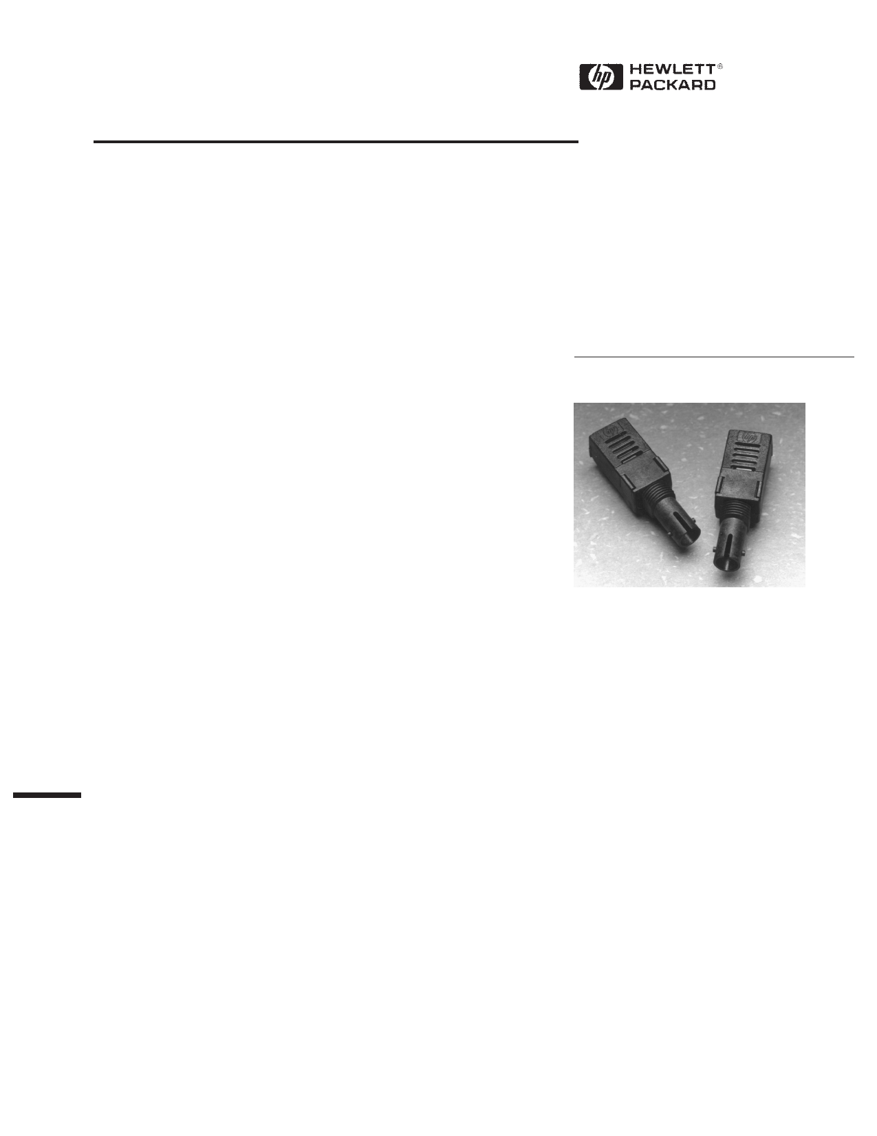
Fiber Optic Transmitter
and Receiver Data Links
for 125 MBd
Technical Data
HFBR-1115T Transmitter
HFBR-2115T Receiver
Features
• Full Compliance with the
Optical Performance
Requirements of the FDDI
PMD Standard
• Full Compliance with the
Optical Performance
Requirements of the ATM
100 Mbps Physical Layer
• Full Compliance with the
Optical Performance
Requirements of the
100 Mbps Fast Ethernet
Physical Layer
• Other Versions Available for:
- ATM
- Fibre Channel
• Compact 16-pin DIP Package
with Plastic ST* Connector
• Wave Solder and Aqueous
Wash Process Compatible
Package
• Manufactured in an ISO
9001 Certified Facility
Applications
• FDDI Concentrators,
Bridges, Routers, and
Network Interface Cards
• 100 Mbps ATM Interfaces
• Fast Ethernet Interfaces
• General Purpose, Point-to-
Point Data Communications
• Replaces DLT/R1040-ST1
Model Transmitters and
Receivers
Description
The HFBR-1115/-2115 series of
data links are high-performance,
cost-efficient, transmitter and
receiver modules for serial
optical data communication
applications specified at 100
Mbps for FDDI PMD or 100 Base-
FX Fast Ethernet applications.
These modules are designed for
50 or 62.5 µm core multi-mode
optical fiber and operate at a
nominal wavelength of 1300 nm.
They incorporate our high-
performance, reliable, long-
wavelength, optical devices and
proven circuit technology to give
long life and consistent
performance.
Transmitter
The transmitter utilizes a
1300 nm surface-emitting
InGaAsP LED, packaged in an
optical subassembly. The LED is
dc-coupled to a custom IC which
converts differential-input, PECL
logic signals, ECL-referenced
(shifted) to a +5 V power supply,
into an analog LED drive current.
Receiver
The receiver utilizes an InGaAs
PIN photodiode coupled to a
custom silicon transimpedance
*ST is a registered trademark of AT&T Lightguide Cable Connectors.
5965-3481E (8/96)
preamplifier IC. The PIN-
preamplifier combination is ac-
coupled to a custom quantizer IC
which provides the final pulse
shaping for the logic output and
the Signal Detect function. Both
the Data and Signal Detect
Outputs are differential. Also,
both Data and Signal Detect
Outputs are PECL compatible,
ECL-referenced (shifted) to a
+5 V power supply.
Package
The overall package concept for
the Data Links consists of the
following basic elements: two
optical subassemblies, two
electrical subassemblies, and the
outer housings as illustrated in
Figure 1.
177
1 page 
Care should be taken to avoid
shorting the receiver Data or
Signal Detect Outputs directly to
ground without proper current-
limiting impedance.
Solder and Wash Process
Compatibility
The transmitter and receiver are
delivered with protective process
caps covering the individual ST*
ports. These process caps protect
the optical subassemblies during
wave solder and aqueous wash
processing and act as dust covers
during shipping.
These data link modules are
compatible with either industry
standard wave- or hand-solder
processes.
Shipping Container
The data link modules are
packaged in a shipping container
designed to protect it from
mechanical and ESD damage
during shipment or storage.
Board Layout–Interface
Circuit and Layout
Guidelines
It is important to take care in the
layout of your circuit board to
achieve optimum performance
from these data link modules.
Figure 7 provides a good example
of a power supply filter circuit that
works well with these parts. Also,
suggested signal terminations for
the Data, Data-bar, Signal Detect
and Signal Detect-bar lines are
shown. Use of a multilayer,
ground-plane printed circuit board
will provide good high-frequency
+5 Vdc
GND
DATA
DATA
Tx Rx
*
A
L2
1
C2
0.1
R3 R2 R4 R1
82 82 130 130
9 NC
10 GND
11 VCC
12 VCC
13 GND
14 D
15 D
16 NC
NC 8
NO
PIN
7
GND 6
GND 5
GND 4
GND 3
VBB 2
NC 1
*
C5
0.1
TERMINATE D, D
AT Tx INPUTS
* 9 NC
NC 8 *
10
NO
PIN
GND 7
11 GND VCC 6
L1
1
12 GND
13 GND
VCC 5
VCC 4
C1 C7
C3
0.1 10
0.1
(OPTIONAL)
C4
10
14 SD
D3
15 SD
16
NO
PIN
D2
NC 1
R7 R5 R8 R6
82 82 130 130
C6
0.1 R9
82
R11
82
TOP VIEWS
R10 R12
130 130
SD
A
DATA
DATA
SD
TERMINATE D, D, SD, SD AT
INPUTS OF FOLLOW-ON DEVICES
NOTES:
1. RESISTANCE IS IN OHMS. CAPACITANCE IS IN MICROFARADS. INDUCTANCE IS IN MICROHENRIES.
2. TERMINATE TRANSMITTER INPUT DATA AND DATA-BAR AT THE TRANSMITTER INPUT PINS. TERMINATE THE RECEIVER OUTPUT DATA, DATA-BAR, AND SIGNAL DETECT-
BAR AT THE FOLLOW-ON DEVICE INPUT PINS. FOR LOWER POWER DISSIPATION IN THE SIGNAL DETECT TERMINATION CIRCUITRY WITH SMALL COMPROMISE TO THE
SIGNAL QUALITY, EACH SIGNAL DETECT OUTPUT CAN BE LOADED WITH 510 OHMS TO GROUND INSTEAD OF THE TWO RESISTOR, SPLIT-LOAD PECL TERMINATION
SHOWN IN THIS SCHEMATIC.
3. MAKE DIFFERENTIAL SIGNAL PATHS SHORT AND OF SAME LENGTH WITH EQUAL TERMINATION IMPEDANCE.
4. SIGNAL TRACES SHOULD BE 50 OHMS MICROSTRIP OR STRIPLINE TRANSMISSION LINES. USE MULTILAYER, GROUND-PLANE PRINTED CIRCUIT BOARD FOR BEST HIGH-
FREQUENCY PERFORMANCE.
5. USE HIGH-FREQUENCY, MONOLITHIC CERAMIC BYPASS CAPACITORS AND LOW SERIES DC RESISTANCE INDUCTORS. RECOMMEND USE OF SURFACE-MOUNT COIL
INDUCTORS AND CAPACITORS. IN LOW NOISE POWER SUPPLY SYSTEMS, FERRITE BEAD INDUCTORS CAN BE SUBSTITUTED FOR COIL INDUCTORS. LOCATE POWER
SUPPLY FILTER COMPONENTS CLOSE TO THEIR RESPECTIVE POWER SUPPLY PINS. C7 IS AN OPTIONAL BYPASS CAPACITOR FOR IMPROVED, LOW-FREQUENCY NOISE
POWER SUPPLY FILTER PERFORMANCE.
6. DEVICE GROUND PINS SHOULD BE DIRECTLY AND INDIVIDUALLY CONNECTED TO GROUND.
7. CAUTION: DO NOT DIRECTLY CONNECT THE FIBER-OPTIC MODULE PECL OUTPUTS (DATA, DATA-BAR, SIGNAL DETECT, SIGNAL DETECT-BAR, VBB) TO GROUND WITHOUT
PROPER CURRENT LIMITING IMPEDANCE.
8. (*) OPTIONAL METAL ST OPTICAL PORT TRANSMITTER AND RECEIVER MODULES WILL HAVE PINS 8 AND 9 ELECTRICALLY CONNECTED TO THE METAL PORT ONLY AND
NOT CONNECTED TO THE INTERNAL SIGNAL GROUND.
Figure 7. Recommended Interface Circuitry and Power Supply Filter Circuits.
181
5 Page 
Notes:
1. This is the maximum voltage that can
be applied across the Differential
Transmitter Data Inputs to prevent
damage to the input ESD protection
circuit.
2. The outputs are terminated with 50 Ω
connected to VCC - 2 V.
3. The specified signaling rate of
10 MBd to 125 MBd guarantees
operation of the transmitter and
receiver link to the full conditions
listed in the FDDI Physical Layer
Medium Dependent standard.
Specifically, the link bit-error-ratio
will be equal to or better than 2.5 x
10-10 for any valid FDDI pattern. The
transmitter section of the link is
capable of dc to 125 MBd. The
receiver is internally ac-coupled
which limits the lower signaling rate
to 10 MBd. For purposes of
definition, the symbol rate (Baud),
also called signaling rate, fs, is the
reciprocal of the symbol time. Data
rate (bits/sec) is the symbol rate
divided by the encoding factor used
to encode the data (symbols/bit).
4. The power supply current needed to
operate the transmitter is provided to
differential ECL circuitry. This
circuitry maintains a nearly constant
current flow from the power supply.
Constant current operation helps to
prevent unwanted electrical noise
from being generated and conducted
or emitted to neighboring circuitry.
5. This value is measured with an output
load RL = 10 kΩ.
6. This value is measured with the out-
puts terminated into 50 Ω connected
to VCC - 2 V and an Input Optical
Power level of -14 dBm average.
7. The power dissipation value is the
power dissipated in the transmitter
and receiver itself. Power dissipation
is calculated as the sum of the
products of supply voltage and
currents, minus the sum of the
products of the output voltages and
currents.
8. This value is measured with respect to
VCC with the output terminated into
50 Ω connected to VCC - 2 V.
9. The output rise and fall times are
measured between 20% and 80%
levels with the output connected to
VCC - 2 V through 50 Ω.
10. Duty Cycle Distortion contributed by
the receiver is measured at the 50%
threshold using an IDLE Line State,
125 MBd (62.5 MHz square-wave),
input signal. The input optical power
level is -20 dBm average. See
Application Information–Data Link
Jitter Section for further information.
11. Data Dependent Jitter contributed by
the receiver is specified with the
FDDI DDJ test pattern described in
the FDDI PMD Annex A.5. The input
optical power level is -20 dBm
average. See Application
Information–Data Link Jitter Section
for further information.
12. Random Jitter contributed by the
receiver is specified with an IDLE
Line State, 125 MBd (62.5 MHz
square-wave), input signal. The input
optical power level is at the maxi-
mum of “PIN Min. (W).” See Applica-
tion Information–Data Link Jitter
Section for further information.
13. These optical power values are
measured with the following
conditions:
• The Beginning of Life (BOL) to the
End of Life (EOL) optical power
degradation is typically 1.5 dB per
the industry convention for long
wavelength LEDs. The actual
degradation observed in Hewlett-
Packard’s 1300 nm LED products
is < 1dB, as specified in this data
sheet.
• Over the specified operating
voltage and temperature ranges.
• With HALT Line State, (12.5 MHz
square-wave), input signal.
• At the end of one meter of noted
optical fiber with cladding modes
removed.
The average power value can be
converted to a peak power value by
adding 3 dB. Higher output optical
power transmitters are available on
special request.
14. The Extinction Ratio is a measure of
the modulation depth of the optical
signal. The data “0” output optical
power is compared to the data “1”
peak output optical power and
expressed as a percentage. With the
transmitter driven by a HALT Line
State (12.5 MHz square-wave) signal,
the average optical power is
measured. The data “1” peak power is
then calculated by adding 3 dB to the
measured average optical power. The
data “0” output optical power is
found by measuring the optical
power when the transmitter is driven
by a logic “0” input. The extinction
ratio is the ratio of the optical power
at the “0” level compared to the
optical power at the “1” level
expressed as a percentage or in
decibels.
15. The transmitter provides compliance
with the need for Transmit_Disable
commands from the FDDI SMT layer
by providing an Output Optical
Power level of <-45 dBm average in
response to a logic “0” input. This
specification applies to either 62.5/
125 µm or 50/125 µm fiber cables.
16. This parameter complies with the
FDDI PMD requirements for the
tradeoffs between center wavelength,
spectral width, and rise/fall times
shown in Figure 9.
17. This parameter complies with the
optical pulse envelope from the FDDI
PMD shown in Figure 10. The optical
rise and fall times are measured from
10% to 90% when the transmitter is
driven by the FDDI HALT Line State
(12.5 MHz square-wave) input signal.
18. Duty Cycle Distortion contributed by
the transmitter is measured at a 50%
threshold using an IDLE Line State,
125 MBd (62.5 MHz square-wave),
input signal. See Application
Information–Data Link Jitter Per-
formance Section of this data sheet
for further details.
19. Data Dependent Jitter contributed by
the transmitter is specified with the
FDDI test pattern described in FDDI
PMD Annex A.5. See Application
Information–Data Link Jitter
Performance Section of this data
sheet for further details.
20. Random Jitter contributed by the
transmitter is specified with an IDLE
Line State, 125 MBd (62.5 MHz
square-wave), input signal. See
Application Information–Data Link
Jitter Performance Section of this
data sheet for further details.
21. This specification is intended to
indicate the performance of the
receiver when Input Optical Power
signal characteristics are present per
the following definitions. The Input
Optical Power dynamic range from
the minimum level (with a window
time-width) to the maximum level is
the range over which the receiver is
guaranteed to provide output data
with a Bit-Error-Ratio (BER) better
than or equal to 2.5 x 10⁻¹⁰.
• At the Beginning of Life (BOL).
• Over the specified operating
voltage and temperature ranges.
• Input symbol pattern is the FDDI
test pattern defined in FDDI PMD
Annex A.5 with 4B/5B NRZI
encoded data that contains a duty-
cycle base-line wander effect of
187
11 Page | ||
| Páginas | Total 12 Páginas | |
| PDF Descargar | [ Datasheet HFBR-2115T.PDF ] | |
Hoja de datos destacado
| Número de pieza | Descripción | Fabricantes |
| HFBR-2115T | Fiber Optic Transmitter and Receiver Data Links for 125 MBd | Agilent(Hewlett-Packard) |
| Número de pieza | Descripción | Fabricantes |
| SLA6805M | High Voltage 3 phase Motor Driver IC. |
Sanken |
| SDC1742 | 12- and 14-Bit Hybrid Synchro / Resolver-to-Digital Converters. |
Analog Devices |
|
DataSheet.es es una pagina web que funciona como un repositorio de manuales o hoja de datos de muchos de los productos más populares, |
| DataSheet.es | 2020 | Privacy Policy | Contacto | Buscar |